
In the high-stakes world of industrial automation, your machine vision camera is only as good as the printed circuit board driving it. As data rates climb and environmental demands intensify, engineers must navigate complex trade-offs between material performance, thermal dissipation, and signal fidelity. This guide provides the strategic framework necessary to ensure your designs survive the factory floor while delivering precision imaging.
The Impact of Substrate Choice on High-Speed Signals

The Impact of Substrate Choice on High-Speed Signals
In high-speed machine vision applications, the PCB substrate is not merely a structural carrier but a critical component of the transmission line. The dielectric constant (Dk) dictates signal propagation speed, while the dissipation factor (Df) governs dielectric loss. For interfaces like MIPI CSI-2, CoaXPress, or 10GbE, minimizing these parameters is crucial to preserve high-frequency signal components, prevent inter-symbol interference (ISI), and reduce jitter.
Evaluating Dielectric Constants and Dissipation
Material selection significantly alters the impedance profile and attenuation characteristics of high-speed traces. FR-4, while cost-effective, typically exhibits higher Df and frequency-dependent Dk instability, which can lead to unacceptable phase distortion in multi-gigabit data streams.
| Material Class | Dk (at 10GHz) | Df (Loss Tangent) | Primary Application |
|---|---|---|---|
| Standard FR-4 | 4.5 - 4.8 | 0.020 | Low-speed control/logic |
| High-Tg / Improved FR-4 | 3.8 - 4.2 | 0.008 - 0.012 | Standard industrial vision |
| PTFE / Ceramic-Filled | 2.2 - 3.5 | < 0.003 | High-speed serialized data |
Key Considerations for Material Selection
- How does Df affect signal integrity?
A high dissipation factor (Df) causes significant energy absorption by the dielectric material as heat, leading to rapid signal attenuation at high frequencies, which closes the eye diagram. - Why is Dk stability important?
Dielectric constant (Dk) stability across frequencies and temperatures ensures predictable impedance control, which is vital for preventing reflections in high-bandwidth camera interfaces. - When should I move away from FR-4?
Engineers should transition to low-loss laminates when trace lengths exceed 3-4 inches or when operating frequencies exceed 5GHz, particularly for uncompressed high-resolution video streams.
Achieving Precise Controlled Impedance
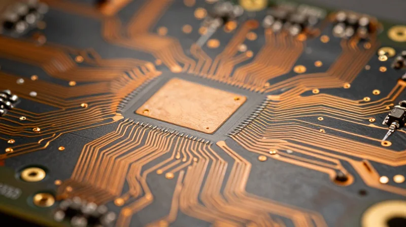
In industrial machine vision, the high-speed data throughput required for real-time image processing makes impedance control a non-negotiable design constraint. Any deviation from the target impedance—typically 90 ohms for USB 3.0 or 100 ohms for LVDS/Ethernet—creates signal reflections that degrade eye diagrams and increase bit error rates. Maintaining precise control requires a synergistic approach involving stack-up planning, material selection, and sophisticated trace geometry calculations.
Critical Factors in Impedance Consistency
| Design Element | Impact on Impedance | Control Recommendation |
|---|---|---|
| Trace Width | Inverse Relationship | Strict adherence to ±5% manufacturing tolerance. |
| Dielectric Thickness | Direct Relationship | Use laser-direct imaging (LDI) for tighter registration. |
| Copper Weight | Profile Variability | Specify VLP (Very Low Profile) copper to minimize etch side-wall effects. |
Best Practices for Trace Design
- How do I account for the glass weave effect?
The variation in Dk due to the glass cloth (the 'fiber weave effect') causes skew. Use spread-glass or flat-glass laminates to ensure consistent dielectric properties along the signal path. - Is reference plane continuity necessary?
Absolutely. Impedance is dependent on the return path. Avoid crossing splits or gaps in the reference plane, as these create inductive discontinuities that cause severe impedance mismatches. - How should I calculate trace width?
Never rely solely on software rule-of-thumb calculators. Collaborate with your PCB fabricator to perform a field solver analysis that accounts for their specific etching processes and manufacturing tolerances.
Advanced engineers should also consider the impact of surface finishes. Finishes like ENIG or Immersion Silver can introduce subtle variations in impedance due to their chemical properties and thickness. For ultra-high-speed machine vision interfaces exceeding 10Gbps, opting for an optimized surface finish and minimizing the use of vias is critical. When vias are unavoidable, ensure they are back-drilled to remove stubs, which act as antennas and significantly disrupt impedance stability at high frequencies.
Advanced Thermal Management Strategies
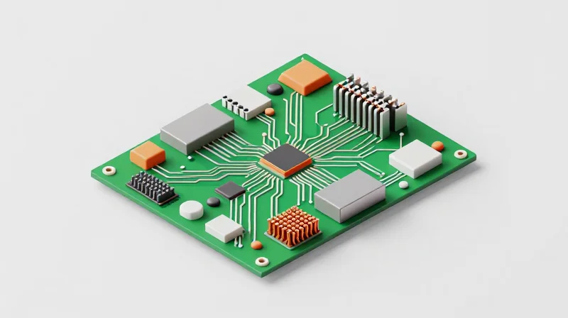
Advanced Thermal Management Strategies
In high-performance machine vision systems, the synergy between processing power and compact physical footprints necessitates aggressive heat dissipation. Thermal management is not merely a post-design afterthought but a foundational requirement that influences material selection, routing density, and layer stack-up configuration to prevent localized hot spots that can degrade semiconductor longevity and signal integrity.
Optimizing PCB Stack-up for Thermal Conductivity
The internal architecture of the PCB acts as the primary heat sink for surface-mount components. By utilizing high thermal conductivity prepregs and maximizing the thickness of internal power and ground planes, engineers can create a low-impedance thermal path. Incorporating heavy copper (2 oz or greater) on internal layers significantly improves lateral heat spreading, which is critical when processors or FPGA modules are located in constrained spaces.
| Strategy | Thermal Benefit | Design Trade-off |
|---|---|---|
| Thermal Vias | Vertical heat conduction to ground planes | Requires increased board surface area |
| Heavy Copper (2oz+) | Superior lateral heat dissipation | Higher fabrication costs and trace width limits |
| Thermal Pads | Direct component-to-plane connection | Increased assembly complexity |
Implementation of Thermal Via Arrays
Thermal via arrays are the most effective method for drawing heat away from high-power components like Image Signal Processors (ISPs). To optimize effectiveness, these vias should be placed directly beneath the thermal pads of the component and connected to solid internal ground planes. For maximum efficiency, utilize copper-filled, capped vias to prevent solder wicking and provide a continuous metal path through the board thickness.
- How does copper weight influence thermal performance?
Increased copper weight decreases the thermal resistance of the trace or plane, allowing for faster heat dispersion across the entire PCB surface area. - Why is thermal via plating important?
Robust plating thickness ensures the via does not become a thermal bottleneck; inadequate plating will significantly restrict the total thermal conductivity of the path. - Can thermal management affect signal integrity?
Yes, excessive via density can disrupt return paths; therefore, thermal layouts must be cross-referenced with impedance-controlled routing to avoid unintended EMI or reflection issues.
Ensuring Electromagnetic Compatibility (EMC)
Best Practices for EMI Mitigation
Industrial environments are characterized by heavy machinery, high-voltage motors, and variable frequency drives, all of which generate substantial electromagnetic interference (EMI). To maintain signal integrity for high-speed camera interfaces like CoaXPress or 10GigE, engineers must treat the PCB as an integrated electromagnetic system rather than just a collection of components.
- Ground Plane Integrity
Utilize solid, uninterrupted ground planes for high-speed signal layers. Avoid splitting ground planes, as this forces return currents to take indirect paths, significantly increasing loop area and EMI emissions. - Differential Pair Shielding
Route sensitive high-speed signals as tightly coupled differential pairs. Implement ground stitching vias alongside these traces to provide a low-inductance return path, effectively containing electromagnetic fields. - Component Partitioning
Physically separate the noisy power conversion and motor control circuitry from the sensitive analog front-end (AFE) and high-speed data processors to prevent cross-talk through substrate coupling.
Comparison of EMI Mitigation Strategies
| Strategy | Primary Function | Implementation Complexity |
|---|---|---|
| Stitching Vias | Reduces return path loop area | Low |
| Buried Vias/Blind Vias | Reduces via stub resonance | High |
| Faraday Cages | Shields sensitive RF/AFE sections | Medium |
| Common Mode Chokes | Filters high-frequency noise from cables | Low |
Frequently Asked Questions on EMC Design
- How do I handle high-speed signal transitions between layers?
Always place a stitching via near the signal transition via to maintain a continuous, low-impedance return path for the high-frequency current component. - Should I pour copper on external layers?
If you utilize external copper pours, ensure they are connected to the main ground plane using a high density of stitching vias to prevent them from acting as unintended antennas.
Selecting Materials for Environmental Durability

Evaluating Material Properties for Harsh Environments
In industrial machine vision, the PCB substrate serves as the foundation for both electrical performance and mechanical survival. Standard FR-4 often fails when subjected to the rapid thermal cycling, constant high-frequency vibration, and chemical exposure typical of automated production lines. Engineers must prioritize materials with high Glass Transition Temperatures (Tg), low Coefficient of Thermal Expansion (CTE), and superior Dielectric Strength to prevent board warping, solder joint fatigue, and delamination.
| Material Type | Key Advantage | Best Use Case |
|---|---|---|
| High-Tg FR-4 (170°C+) | Improved thermal stability | General industrial automation |
| Polyimide | Flexibility & high heat tolerance | Robotic arms and moving parts |
| Ceramic-Filled PTFE | Low loss and low CTE | High-speed data & high-frequency imaging |
| Metal-Core PCB | Extreme heat dissipation | High-intensity lighting & power LED arrays |
Addressing Mechanical and Thermal Stressors
Mechanical durability is as vital as thermal resilience. Machine vision systems mounted on CNC machines or robotic platforms experience harmonic vibrations that can cause copper cracking. Selecting materials with a low z-axis CTE is essential to keep vias intact through thousands of thermal cycles. Furthermore, environmental sealing (conformal coating) should be treated as a secondary material choice that works in tandem with the substrate to block oils, solvents, and corrosive particulates.
Critical Selection FAQs
- Why is the Glass Transition Temperature (Tg) so critical?
Tg is the temperature where the PCB material transitions from a rigid state to a softer, more rubber-like state. Exceeding this value can cause significant reliability failures including via barrel cracking and delamination. - How does moisture absorption affect high-speed vision data?
Materials that absorb moisture see a shift in dielectric constant (Dk), which leads to impedance mismatches. In high-speed LVDS or SerDes interfaces, this manifests as signal jitter and dropped video frames. - Should I opt for halogen-free laminates?
Yes, especially if the machine vision unit is placed in sealed, compact enclosures. Halogen-free materials produce less toxic smoke in the event of component failure and often offer better thermal stability for modern high-density designs.
Layout Best Practices for Noise Immunity
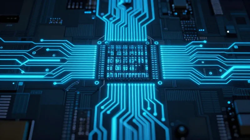
Strategic Partitioning and Isolation
The foundation of noise immunity in high-performance machine vision is the physical and electrical separation of circuitry. In an industrial environment, the CMOS image sensor is highly susceptible to interference from high-speed digital processing (FPGAs/SoCs) and switching power supplies. By maintaining distinct 'islands' for analog and digital grounds—connected only at a single star-point—engineers can prevent return currents from noisy digital components from corrupting the delicate analog ground reference.
Layout Techniques for Noise Mitigation
| Layout Strategy | Noise Impact | Engineering Benefit |
|---|---|---|
| Differential Signaling | Low | Superior common-mode noise rejection. |
| Component Guard Rings | Low | Reduces leakage current in sensitive nodes. |
| Via Stitching | Medium | Stabilizes ground planes for reduced EMI. |
Key Questions for Noise-Resilient Design
- How does stack-up configuration influence noise immunity?
A high-performance stack-up should prioritize solid ground planes directly beneath high-speed signals to minimize loop area and provide a controlled impedance path for return currents. - Can trace routing mitigate cross-talk in machine vision?
Yes, maintaining a '3W' rule—spacing traces at least three times the trace width apart—significantly reduces capacitive coupling between high-speed signal lines and sensitive analog inputs. - What role does shielding play in industrial camera boards?
Integrated board-level shielding (BLS) acts as a physical barrier to radiated emissions, effectively containing noise generated by high-frequency clock oscillators and switching converters.
Ultimately, the layout process must prioritize the shortest path for return currents. When signals must traverse different layers, stitching vias must be placed adjacent to signal vias to maintain the integrity of the reference plane and prevent ground bounce, which is often the primary culprit behind intermittent image artifacts and pixel noise in industrial applications.
Regulatory Compliance and Industry Standards
Adhering to IPC and Global Compliance Standards
In industrial machine vision, PCBs are subjected to rigorous operational demands that necessitate strict adherence to international standards. Compliance is not merely a legal hurdle but a benchmark for quality assurance and interoperability. Designers must prioritize IPC-6012 and IPC-A-600 standards, which define the acceptability and qualification of rigid printed boards, ensuring that solder joints and interconnects can withstand the mechanical stress of constant machine vibration.
| Standard | Focus Area | Industrial Impact |
|---|---|---|
| IPC-6012 | Board Performance | Ensures structural integrity under thermal/vibration stress. |
| RoHS | Hazardous Substances | Mandatory lead-free compliance for EU/global market entry. |
| REACH | Chemical Safety | Regulates chemical usage to ensure worker and environmental safety. |
| UL 94V-0 | Flammability | Critical safety rating for industrial enclosures and high-power boards. |
Key Regulatory Considerations for Machine Vision
- Why is RoHS compliance critical for vision systems?
Beyond legal mandates, RoHS compliance ensures that the materials used in your PCB do not degrade prematurely due to oxidation or thermal cycling, which is common in high-heat vision processing environments. - How does UL certification affect machine deployment?
Many industrial facilities require UL-certified hardware for insurance and safety inspections; utilizing UL-recognized laminate materials avoids costly redesigns during the final machine integration phase. - Is IPC Class 3 necessary for my machine vision PCB?
IPC Class 3 is reserved for high-reliability electronics where equipment downtime is unacceptable; if your vision system is part of a mission-critical line, Class 3 manufacturing standards are highly recommended.
Designers should maintain a 'Compliance-by-Design' approach. This includes documenting material stack-ups that meet environmental regulations, ensuring that all outsourced assembly partners are certified to IPC-J-STD-001 requirements. Proactive management of these standards reduces the risk of expensive product recalls and ensures that your industrial vision platform can be deployed globally without restrictive market barriers.
Selecting the optimal PCB architecture is the foundation of high-performance machine vision. By balancing advanced material science with rigorous layout discipline, you can guarantee both data integrity and hardware longevity. Ready to elevate your next project? Contact our engineering team today to discuss your specific PCB requirements and accelerate your time-to-market.
