The backbone of today's cutting-edge electronics is the printed circuit board (PCB). As technology advances, the need for reliable and high-performance PCBs becomes more critical. High tech PCB manufacturers are not just assembly lines but crucial partners in innovation. This article provides a comprehensive guide to help you navigate the complexities of selecting the right high tech PCB manufacturer, ensuring your project's success through a combination of the latest tech and best practices.
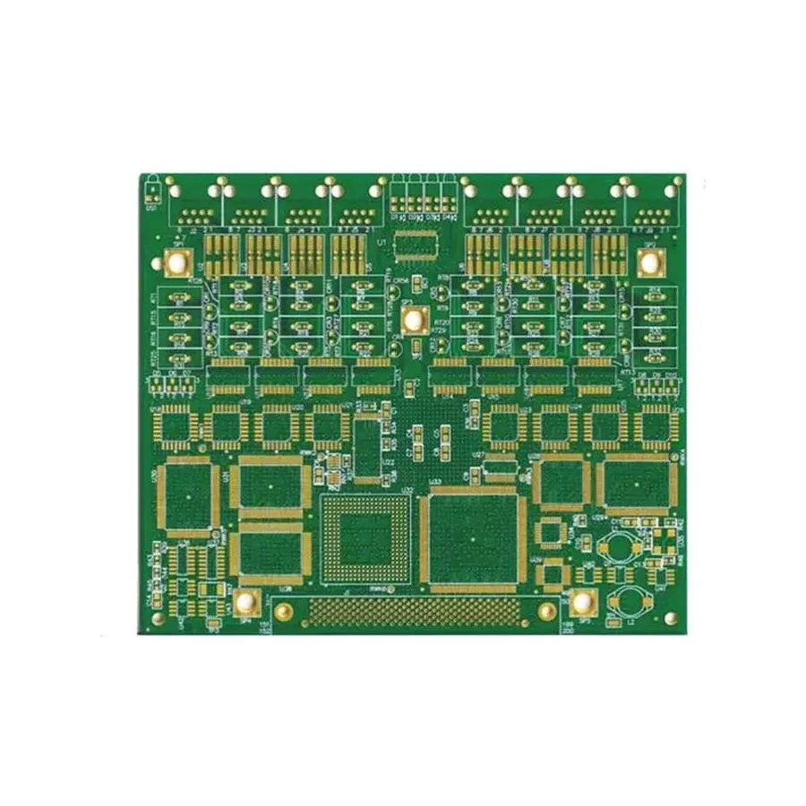
Before engaging a high-tech PCB manufacturer, a thorough understanding of your project's specific requirements is paramount. This foundational step ensures that the selected manufacturer possesses the necessary capabilities and expertise to meet your design specifications, ultimately leading to a successful and reliable end-product.
Selecting the appropriate high-tech PCB manufacturer requires a thorough evaluation of several crucial factors. These considerations extend beyond mere cost and encompass the manufacturer's capabilities, technological expertise, quality commitment, and adherence to industry standards. A meticulous review ensures the chosen partner can consistently meet the demands of your project.
| Factor | Description | Importance |
|---|---|---|
| Manufacturing Capabilities | Assess the range of PCBs they can produce, including layer count, size, and complexity. Look for quick-turn prototyping services. | Ensures the manufacturer can handle your specific project needs and deliver prototypes rapidly. |
| Material Expertise | Evaluate their experience with different materials (e.g., FR-4, high-speed laminates, flexible substrates) and their ability to handle advanced materials. | Guarantees the use of appropriate materials for your application, affecting performance and reliability. |
| Technological Proficiency | Determine their capabilities with advanced technologies like HDI (High-Density Interconnect), microvias, and embedded components. | Confirms they have the tools and expertise to manage intricate PCB designs. |
| Quality Standards | Check for certifications like ISO 9001, UL, and IPC compliance, as well as internal quality control procedures. | Assures consistent production quality and conformity to industry benchmarks. |
| Certification Compliance | Verify if they can provide necessary certifications for your industry or application (e.g., medical, aerospace). | Ensures legal and industry compliance, reducing risks associated with non-certified products. |
| Pricing Structure | Understand their pricing model for prototype and production quantities, as well as any hidden costs. | Impacts the overall project budget, making transparency critical. |
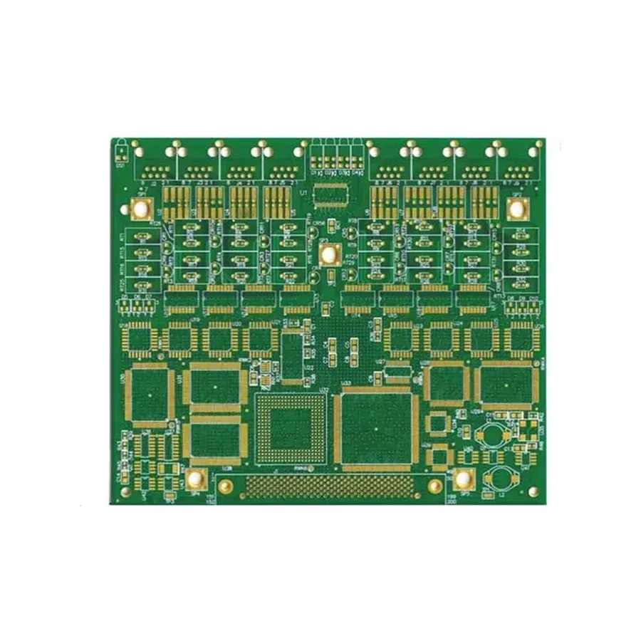
Selecting the right high-tech PCB manufacturer is crucial for project success. This section provides a comparative analysis of leading manufacturers, examining their strengths, limitations, geographical presence, and specialized areas. This analysis will help you identify a manufacturer that aligns with your project’s specific requirements and technological demands.
| Manufacturer | Strengths | Limitations | Geographic Focus | Specialization |
|---|---|---|---|---|
| Hitech Circuits | Strong in quick-turn prototyping, offers a range of materials | May have limited capacity for extremely large volume production | Primarily North America and some presence in Europe. | Rapid prototyping, complex multilayer PCBs, impedance control |
| TTM Technologies | Large global footprint, significant capacity for volume production, advanced technologies including HDI | Can be less flexible for small custom runs and may have higher MOQs | Global presence with manufacturing facilities in North America, Asia, and Europe. | High-volume PCB production, HDI, RF/Microwave PCBs, Aerospace and Defense |
| Multek | Focus on flexible and rigid-flex PCB manufacturing with high reliability, automotive industry expertise | Less emphasis on standard rigid boards, may not be ideal for quick prototyping of rigid PCBs | Global manufacturing locations with strong presence in Asia. | Flexible PCBs, rigid-flex PCBs, high-reliability applications, automotive PCBs. |
| Advanced Circuits | Strong US-based manufacturer with a focus on rapid prototyping and small to medium volume runs | May not be suitable for extreme high volume global manufacturing. | Primarily North America, with focus on serving US market. | Rapid PCB prototyping, quick-turn manufacturing, advanced materials and tight tolerances |
| Amitron | Specialized in high-reliability PCBs and complex constructions | Limited capacity for low-cost, high-volume commodity PCBs. | Primarily based in the United States and serves the North American market. | High reliability PCB, mil-spec and aerospace PCBs, complex boards with advanced materials. |
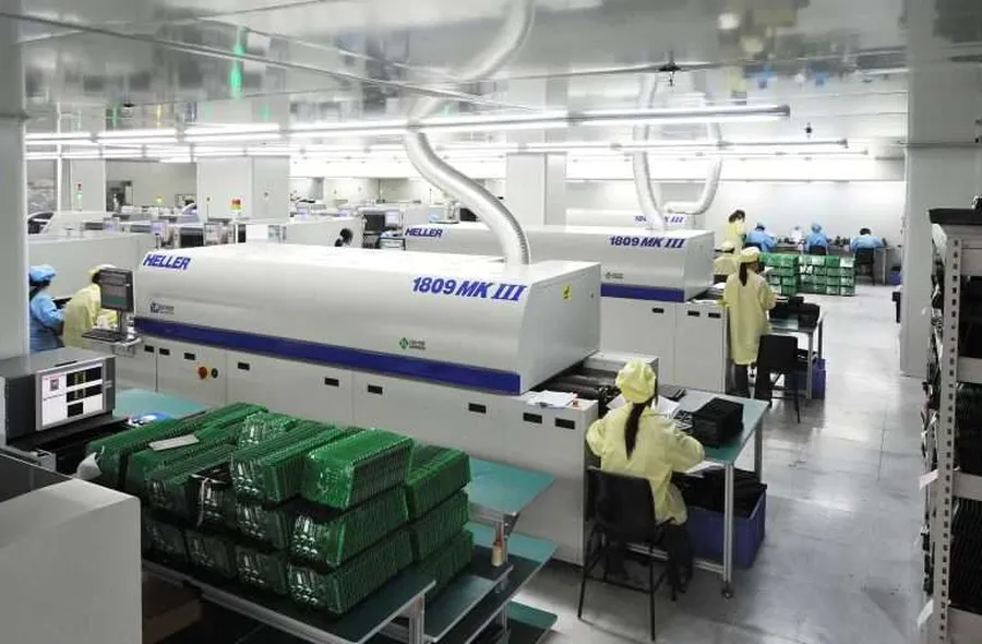
The decision between engaging a local or overseas high-tech PCB manufacturer significantly impacts project outcomes. Evaluating factors such as cost, lead times, communication efficiency, and supply chain complexities is crucial for determining the most suitable partnership.
| Factor | Local Manufacturers | Overseas Manufacturers |
|---|---|---|
| Cost | Generally higher due to labor and overhead costs. | Typically lower due to lower labor costs and economies of scale. |
| Turnaround Time | Faster, especially for prototyping and quick-turn orders. | Longer lead times due to shipping and potential customs delays. |
| Communication | Easier communication due to similar time zones and potentially language. | Can be challenging due to time zone differences and potential language barriers. |
| Intellectual Property Protection | Stronger legal protections and easier enforcement of IP rights. | Greater risk of intellectual property theft or reverse engineering, requiring careful vetting and contract negotiation. |
| Supply Chain | More agile and easier to manage, with less risk of disruptions due to geographical proximity. | Can be complex and vulnerable to disruptions such as shipping delays, customs issues, and geopolitical instability. |
| Quality Control | Easier to conduct site visits and audits. | More challenging to verify quality firsthand; requires thorough documentation review and reliance on certifications. |
| Minimum Order Quantity | May be lower, with flexibility for small batches or prototypes. | Often higher, as overseas factories focus on large-scale production. |
Choosing between a local or overseas manufacturer should be a strategic decision based on the specific needs of your project. Factors such as design complexity, budget constraints, time to market pressures, and the level of required quality control should all be considered.
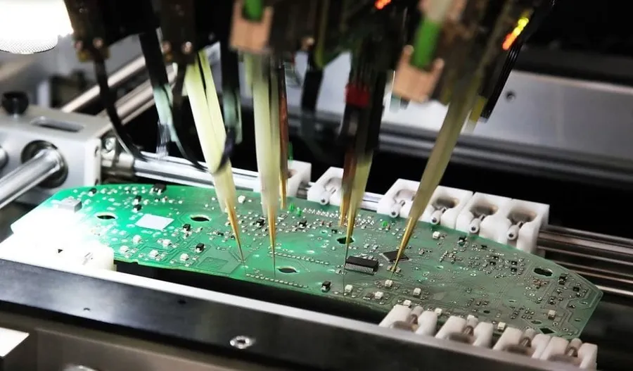
Evaluating a high-tech PCB manufacturer's capabilities requires a deep understanding of their technological proficiency and capacity to meet specific project demands. This involves scrutinizing their equipment, material handling expertise, and experience with diverse PCB types and complexities. A thorough assessment ensures that the chosen manufacturer can deliver high-quality PCBs that align with intricate project requirements.
| Capability Category | Specific Evaluation Criteria | Importance |
|---|---|---|
| PCB Types Supported | Rigid, flexible, rigid-flex, HDI, multilayer PCBs. Assess if they specialize or have experience in your needed type. | High |
| Material Expertise | Experience with FR-4, polyimide, Teflon, and metal core PCBs. Check their knowledge of material properties and selection process. | High |
| Manufacturing Technology | Assess for modern machinery like laser direct imaging, advanced etching processes, and automated assembly lines. Confirm their ability to produce tight tolerances. | High |
| Layer Count Capability | Ability to produce the number of layers your design requires, including any complex stack-ups. Verify the maximum layer count. | High |
| Tolerances and Precision | Inquire about their capabilities to meet precise feature sizes and spacing. Examine their control over track width, spacing, and via dimensions. | High |
| Surface Finish Options | Check for available finishes like ENIG, HASL, immersion tin/silver. Confirm they have expertise in finishes appropriate for your application. | Medium |
| Special Processes | Evaluate experience with special technologies including blind/buried vias, impedance control, and microvia technology. | Medium |
| Testing and Inspection | Capabilities to perform electrical tests, AOI (Automated Optical Inspection), and X-ray analysis. Ensure a complete verification of board quality. | Medium |
| Prototype and Small Batch | Inquire if they offer quick-turn prototype services. Verify their ability to handle small batch production for design iterations. | Medium |
| Project Complexity Handling | Assess experience with projects similar to yours, complex designs, and ability to address intricate design needs. | High |
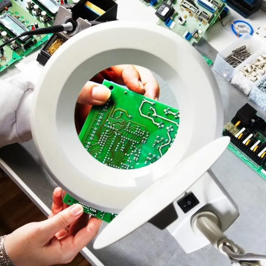
Rigorous quality control and adherence to industry certifications are paramount in high tech PCB manufacturing, ensuring the reliability and performance of electronic products. Certifications such as ISO 9001, UL, and IPC standards are not merely formalities; they represent a commitment to consistent quality and process control across all stages of PCB fabrication.
| Certification | Description | Relevance to PCB Manufacturing |
|---|---|---|
| ISO 9001 | An international standard for quality management systems. | Ensures a consistent approach to manufacturing processes and continuous improvement within the high tech pcb manufacturer. |
| UL | Safety certification by Underwriters Laboratories. | Verifies that the PCBs meet stringent safety standards, particularly critical for high-power applications or use in hazardous environments. |
| IPC Standards (e.g., IPC-A-600) | A set of industry-consensus standards for PCB design, fabrication, and assembly. | Provides clear guidelines on acceptability criteria for PCBs, ensuring consistent quality from board to board. For example, IPC-A-600 dictates the acceptability of PCBs, particularly focusing on attributes visible after fabrication |
These certifications act as a verifiable benchmark, allowing clients to confidently choose high tech PCB manufacturers that meet stringent quality criteria. They reduce the risk of failures and guarantee a higher level of reliability in the final product. Manufacturers that obtain and consistently maintain these certifications demonstrate their dedication to meeting the demanding requirements of modern electronics.
Optimizing costs in high-tech PCB manufacturing requires a strategic approach that balances financial considerations with performance requirements. This involves careful planning from the design phase through material selection and manufacturing processes, ensuring that cost efficiencies are achieved without sacrificing the quality and reliability of the final product. By leveraging smart design choices and value engineering, significant cost reductions can be realized while meeting the project's specifications.
This section addresses common questions regarding high tech PCB manufacturing, offering insights into typical processes, design considerations, and cost factors. These questions aim to provide clarity for those seeking to understand the intricacies of sourcing and working with a high tech PCB manufacturer.
The high tech PCB manufacturing sector is undergoing rapid transformation, driven by advancements in technology and increasing demands for more compact, efficient, and high-performing electronic devices. These trends necessitate manufacturers to innovate and adapt continuously, impacting material usage, manufacturing processes, and automation levels.
Choosing the right high tech PCB manufacturer is critical to your project's success. By thoroughly evaluating your needs, comparing manufacturers, and considering key factors like quality and cost, you can select a partner that provides reliable PCBs that meet your exact requirements. For advanced technological applications, a manufacturer with extensive experience, cutting-edge equipment, and a commitment to high quality like many of today's high tech pcb manufacturer, is essential to deliver high performing and durable electronic products. Partnering with a reliable manufacturer is the bedrock for building tomorrow's technologies.

