In today's rapidly evolving tech landscape, the demand for high-quality yet affordable PCBs is paramount. JLCPCB Factory 3 stands at the forefront, leveraging advanced technologies to transform PCB fabrication. This article delves into their innovative processes, examining how they achieve a balance between cost and quality, while also discussing their PCB assembly and 3D printing services. It's a journey into the heart of modern electronics manufacturing, and how companies like JLCPCB bridge the gap between cutting-edge science and the practical applications we see around us everyday.
JLCPCB Factory 3 Overview: A Modern Manufacturing Powerhouse
JLCPCB Factory Exterior
JLCPCB Factory 3 represents a significant leap in PCB manufacturing capabilities, underscoring JLCPCB's pivotal role in the global electronics supply chain. This state-of-the-art facility is not merely a production site; it is a testament to advanced manufacturing practices, equipped with cutting-edge technology to meet the diverse and evolving needs of the modern electronics industry. The factory's operations are designed for high-volume production while maintaining strict adherence to quality control, ensuring that products meet stringent industry standards.
Advanced PCB Manufacturing Processes at JLCPCB Factory 3
PCB Manufacturing Equipment
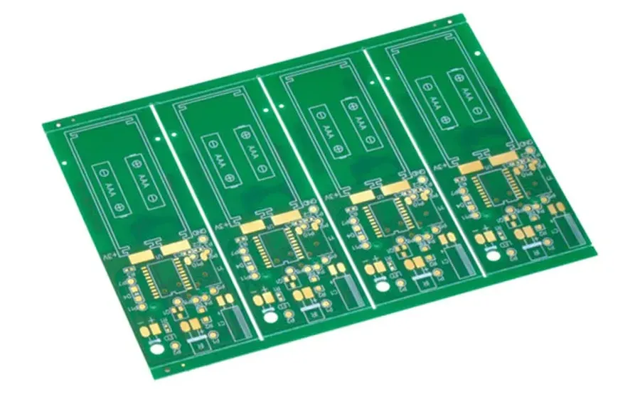
JLCPCB Factory 3 employs a sophisticated, multi-stage process to manufacture high-quality printed circuit boards (PCBs). This process encompasses substrate selection, layer imaging, etching, and finishing, each optimized for precision and efficiency using advanced technologies.
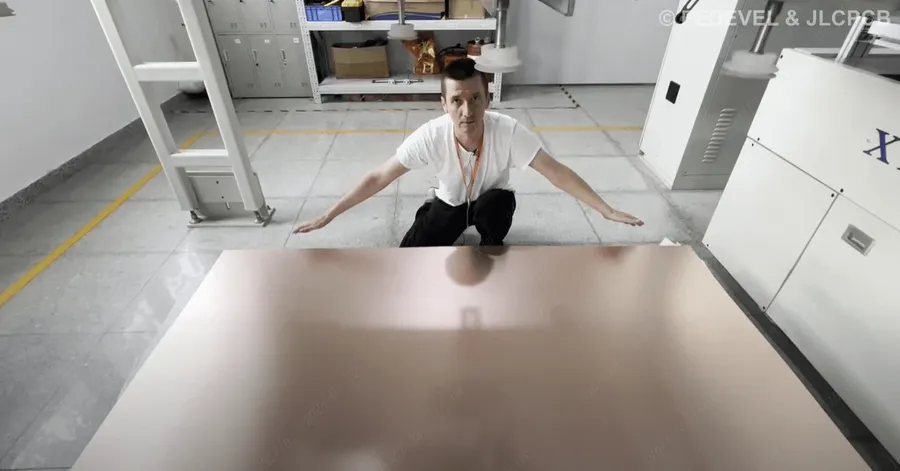
Substrate Selection The process begins with the careful selection of the substrate material, typically FR-4, chosen for its balance of cost, mechanical strength, and electrical properties. Other specialized materials are also available for applications requiring specific performance characteristics such as high-frequency or thermal management.
Layer Imaging Once the substrate is selected, a photosensitive resist is applied to the board surface. The circuit pattern is then transferred onto the board using UV light exposure through a precision photomask, creating the desired circuit layout on the board.
Etching Following imaging, the board is treated with a chemical etching solution. This process removes the exposed copper, leaving behind the desired circuit traces, pads, and vias, thus defining the conductive pathways of the PCB.
Layer Alignment and Lamination For multilayer PCBs, multiple layers undergo imaging and etching before being carefully aligned and laminated together using heat and pressure. This creates a unified multi-layered structure with precise internal connections.
Drilling After lamination, vias and component mounting holes are precisely drilled using computer-controlled drilling machines. These holes allow for electrical connections between different layers and accommodate component leads.
Plating The drilled holes and surface are then subjected to electrochemical plating to deposit a thin layer of copper, ensuring reliable electrical connections and consistent conductivity across the board. This is crucial for both surface mount and through-hole components.
Solder Mask Application A solder mask layer is applied to protect the copper traces and prevent solder bridges during component assembly. The solder mask is cured using UV light, exposing only the pads for soldering.
Silkscreen Printing The final step in PCB fabrication involves printing a silkscreen layer, which includes part numbers, component locations, and other identifying information, facilitating easier assembly and troubleshooting.
Surface Finishing A final surface finish, such as HASL (Hot Air Solder Leveling), ENIG (Electroless Nickel Immersion Gold), or other alternatives are applied to protect the copper and ensure good solderability. The choice of finish depends on the application and design requirements.
Electrical Testing Before moving to the assembly process, each fabricated PCB undergoes rigorous electrical testing to ensure it meets the required specifications and performance standards, detecting any defects or manufacturing flaws.
PCB Assembly Capabilities: Precision and Efficiency
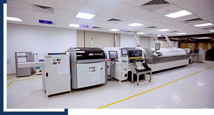
SMT Assembly Line
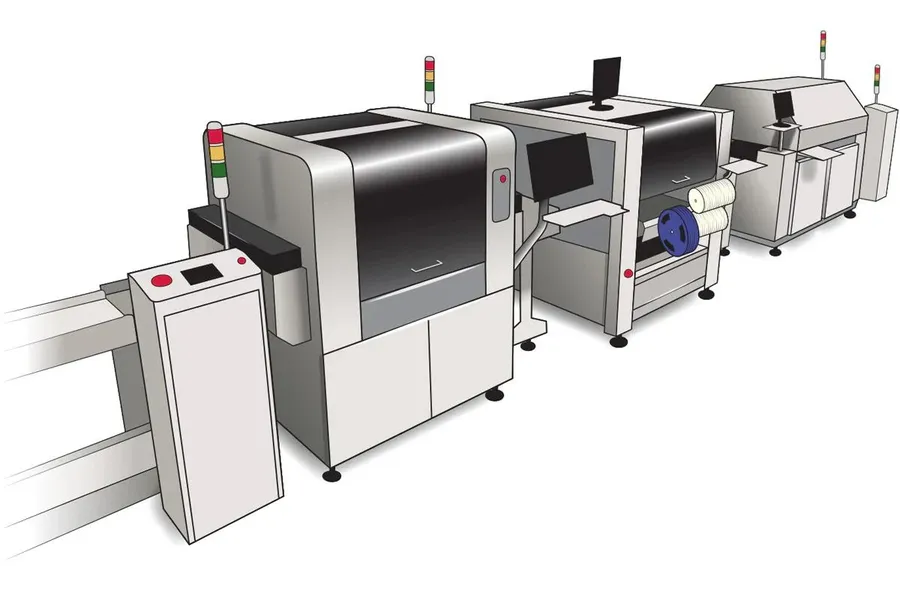
JLCPCB's PCB assembly process is engineered for precision and efficiency, transforming bare PCBs into fully functional electronic modules. This process encompasses a meticulous series of steps, from component preparation to final testing, all designed to meet stringent quality standards.
The PCB assembly process at JLCPCB involves several key stages, each critically important to the overall quality of the final product:
Component Preparation Prior to assembly, all components are carefully inspected and prepared. This may involve cutting component tape reels, baking components to remove moisture, and verifying component values. Automated machines accurately handle and position components, adhering to precise placement parameters to ensure high assembly quality.
Solder Paste Application Solder paste, a mixture of solder alloy and flux, is applied to the PCB pads using stencil printing. The stencil aligns perfectly with the PCB pads, ensuring the precise amount of solder paste is deposited for secure component mounting and electrical connectivity. This process must be exact to avoid soldering defects.
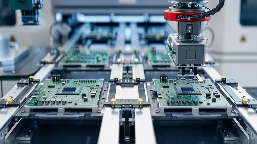
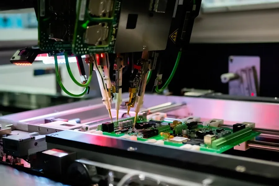
Component Placement Automated pick-and-place machines precisely place surface mount (SMT) components onto the solder paste, using data from the design's bill of materials (BOM) and centroid files. The placement accuracy is critical for reliable electrical connections and proper circuit functioning. The machines are regularly calibrated to maintain high accuracy.
Reflow Soldering After component placement, the assembled PCB goes through a reflow soldering oven. The oven heats the solder paste, causing it to melt and fuse the components to the PCB. Precise temperature control throughout the reflow process ensures that solder joints are strong, reliable, and conform to industry standards. The temperature profile is optimized for the specific components and materials being used to prevent damage.
Through-Hole Component Insertion and Soldering For through-hole components, insertion may be manual or semi-automated, depending on the component's complexity and production volume. These are typically wave soldered, or hand soldered with particular attention to solder quality and alignment. Proper insertion and soldering are essential to ensure stable mechanical and electrical connections.
Inspection and Quality Control Following soldering, each assembled PCB is thoroughly inspected using Automated Optical Inspection (AOI) systems, which compare images of the board against a known good template, and X-ray inspection, which is particularly useful for examining BGA (Ball Grid Array) and other hard-to-inspect component solder joints. These quality control measures catch any assembly defects early, including misalignment, missing components, or improper soldering. Any detected defects trigger corrective actions to ensure final product reliability and performance.
JLCPCB utilizes advanced machinery and strict quality control measures during each assembly phase, guaranteeing precise component placement, reliable solder joints, and overall high assembly quality. This commitment to quality throughout the process ensures that assembled PCBs meet the demanding requirements of modern electronics applications.
The Role of Automation and Technology in JLCPCB Factory 3
Automated PCB Manufacturing
JLCPCB's Factory 3 leverages extensive automation and cutting-edge technologies to ensure consistent, high-quality PCB production. By integrating advanced systems like Solder Paste Inspection (SPI) and automated material handling, JLCPCB achieves precision and efficiency that are crucial for large-scale PCB manufacturing, optimizing production and minimizing defects.
Automated Material Handling Systems Automated guided vehicles (AGVs) and robotic arms are used to transport materials between workstations, reducing manual labor and minimizing handling errors. These systems ensure that components are delivered to the right place at the right time, maintaining a smooth and continuous production flow.
Surface Mount Technology (SMT) Automation Automated SMT lines place components accurately and at high speeds. Pick-and-place machines utilize advanced vision systems to ensure correct component orientation and placement, vital for achieving precise assembly with tight tolerances.
Solder Paste Inspection (SPI) SPI systems are integrated inline to verify the quality and consistency of solder paste deposition. This crucial step helps prevent defects like insufficient solder, excess solder, and bridging, which impact the reliability of the final assembly. By identifying issues early, SPI ensures downstream processes are optimized and reduces the need for rework.
Automated Optical Inspection (AOI) AOI systems use high-resolution cameras to detect manufacturing defects on PCBs after soldering, including missing components, misaligned parts, solder bridges, and open circuits. By providing detailed visual checks, AOI significantly improves the overall quality and reliability of the manufactured boards.
Automated Testing Systems Automated test equipment performs electrical tests to verify that the boards meet all performance criteria. This includes in-circuit testing (ICT) and functional testing, ensuring that only correctly functioning PCBs are shipped to customers.
Cost-Effective PCB Solutions: How JLCPCB Maintains Affordability
PCB Bulk Production
JLCPCB achieves cost-effectiveness in PCB manufacturing through a multifaceted approach that prioritizes efficiency and strategic resource management. This enables them to offer highly competitive pricing without sacrificing the quality and performance of their printed circuit boards.
The core of JLCPCB's cost-effectiveness lies in several key areas:
Economies of Scale JLCPCB’s large-scale operations allow them to reduce per-unit costs significantly. By producing a high volume of PCBs, they benefit from bulk purchasing of materials and optimized production processes, which lower overall expenses.
Vertical Integration By managing many aspects of the production process internally, JLCPCB reduces reliance on external suppliers. This results in minimized costs from reduced transaction fees and improved control over the supply chain, ensuring both affordability and consistent quality.
Advanced Automation Implementation of advanced automation technologies throughout the manufacturing process reduces labor costs, increases throughput, and minimizes the occurrence of human error. Automated systems allow them to produce high-quality PCBs at lower costs per unit.
Efficient Supply Chain Management JLCPCB’s supply chain is structured to reduce waste, optimize logistics, and secure the best material prices. Effective inventory control and just-in-time delivery systems also minimize costs, which results in cost savings being passed to the end consumer.
Technological Innovation Continuous investment in R&D allows JLCPCB to improve manufacturing methods and adopt new techniques which ultimately reduces manufacturing costs through enhanced efficiency and performance.
These combined strategies ensure that JLCPCB can offer competitive pricing while maintaining high standards in PCB manufacturing.
Beyond PCBs: JLCPCB's 3D Printing Services
3D printed parts
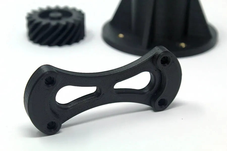
While JLCPCB is primarily known for its printed circuit board (PCB) manufacturing services, the company has expanded its offerings to include 3D printing, providing a complementary service that caters to rapid prototyping and custom mechanical part needs. This expansion allows JLCPCB to serve as a more comprehensive manufacturing partner for its customers.
JLCPCB's 3D printing services leverage various technologies and materials to create functional prototypes and end-use parts. The company's integrated platform allows users to seamlessly transition from PCB design to mechanical enclosure or component prototyping, thereby streamlining product development cycles.
3D Printing Technologies Offered by JLCPCB JLCPCB typically provides a range of 3D printing technologies including Fused Deposition Modeling (FDM), Stereolithography (SLA), and Selective Laser Sintering (SLS), catering to diverse needs.
Materials Available A selection of materials are available, such as PLA, ABS, PETG, and Nylon for FDM; resins for SLA; and PA12, PA12GB for SLS. These options support various applications with different requirements for mechanical strength, temperature resistance, and surface finish.
Applications of JLCPCB 3D Printing The 3D printing service is used for creating enclosures for electronics, prototypes for mechanical parts, jigs and fixtures for assembly, custom tooling, and end-use parts.
Feature
PCB Services
3D Printing Services
Primary Function
Fabrication of circuit boards
Production of three-dimensional objects
Materials
FR-4, Aluminum, etc.
PLA, ABS, Resins, Nylon, etc.
Process
Layer imaging, etching, and plating
Additive manufacturing, building layers upon layers
Application
Electronic circuit integration
Mechanical enclosures, prototypes, custom parts
Typical Use Case
Producing a functional electronics assembly
Rapid prototyping and custom mechanical components
Frequently Asked Questions about JLCPCB's Manufacturing Capabilities
This section addresses common inquiries regarding JLCPCB's manufacturing prowess, offering clear and concise answers to help users understand their capabilities, production processes, and service offerings. We delve into questions about their origin, technical abilities, and competitive standing within the PCB manufacturing industry.
Is JLCPCB a Chinese company? Yes, JLCPCB is a Chinese company with its headquarters and primary manufacturing facilities located in China. This allows them to leverage a robust supply chain and manufacturing infrastructure to provide cost-effective PCB solutions.
Can JLCPCB manufacture PCBs with blind vias? Yes, JLCPCB offers the capability to manufacture PCBs with blind vias. These are vias that connect an outer layer to one or more inner layers, enhancing design flexibility. However, they have certain manufacturing capabilities like minimum via size, aspect ratio, and layer count that may affect the use of blind vias, it's essential to refer to their manufacturing specifications to ensure the design is compliant.
Who is the largest PCB manufacturer in the world? While JLCPCB is a significant player, the title of largest PCB manufacturer changes periodically due to market dynamics. However, companies like TTM Technologies, Zhen Ding Technology, and Unimicron Technology are often cited as some of the largest in terms of revenue and production capacity. JLCPCB distinguishes itself with its rapid prototyping capabilities and low prices.
What is the typical lead time for JLCPCB assembly services? The lead time for JLCPCB assembly services varies depending on the complexity of the PCB, the availability of components, and the quantity of boards ordered. Generally, standard orders take a few days for production with additional time for shipping. Expedited services are available for faster turnaround, which results in an increase in cost. Specific lead times can be confirmed through their online ordering system.
What is the minimum order quantity for JLCPCB's PCB services? JLCPCB is known for offering very low minimum order quantities (MOQ) making them ideal for prototyping and small production runs. For standard PCBs the MOQ is typically 5 pieces for simple boards. They also provide a wide range of options for varying quantities based on specific needs which makes them a flexible manufacturing partner.
Does JLCPCB offer stencil service? Yes, JLCPCB provides stencil services alongside their PCB manufacturing and assembly services. These stencils are crucial for applying solder paste precisely onto the pads before component placement, ensuring the accuracy and consistency for the assembly process.
What PCB design software is compatible with JLCPCB's manufacturing process? JLCPCB is compatible with a variety of PCB design software, including but not limited to Altium Designer, KiCad, Eagle, and EasyEDA, their own design tool. Users need to provide files in standard Gerber format (RS-274X), which most of the PCB design tools support. Additionally they also allow the import of native PCB design files from their supported software simplifying the design review and ordering process.
Feature
JLCPCB
PCBWay
Other Major Competitors
Typical Lead Time
Varies; often rapid prototyping and good delivery times.
Varies; often rapid prototyping and good delivery times.
Can be longer, especially for custom orders
Price
Highly competitive, especially for small orders.
Competitive, with a focus on mid-range options
Varies, with some offering discounts for volume production.
Minimum Order Quantity
Low, starting from 5 pcs for standard PCBs.
Low, similar to JLCPCB in small quantity orders.
Often higher, better suited for large orders
Manufacturing Capabilities
Advanced capabilities including blind vias, multilayer PCBs, and assembly service.
Advanced capabilities comparable to JLCPCB in most aspects
Often specialize in specific high-end technologies or very high volumes
Online Ordering
User-friendly platform with instant quote & order.
User-friendly online platform
Often varies some are user friendly and others are not.
Assembly Services
Yes, SMT and through-hole assembly options available.
Yes, offering assembly services and BOM management.
May offer limited or specialized assembly services
Specialization
Known for rapid prototyping and affordable services.
Known for versatility, rapid prototyping, and a range of services
Specialization in high-end, large-volume PCB manufacturing.
Quality Assurance and Testing at JLCPCB Factory 3
PCB Testing Equipment
JLCPCB implements rigorous quality assurance and testing protocols at Factory 3 to ensure the high reliability and performance of their printed circuit boards. This commitment to quality is paramount, as PCBs are critical components in a wide range of electronic devices, and any defect can lead to system malfunction or failure.
The quality assurance process is multifaceted, encompassing every stage of PCB production from raw material inspection to final product testing. This proactive approach allows JLCPCB to identify and rectify any potential issues early, minimizing waste and maximizing customer satisfaction. This process includes material verification, automated optical inspection (AOI), electrical testing, and functional testing based on client specifications.
Testing Stage
Description
Purpose
Incoming Material Inspection
Verification of raw materials (e.g., copper-clad laminates) against specifications.
Ensures the use of high-quality materials as the base for manufacturing.
Automated Optical Inspection (AOI)
Automated visual examination of PCB layers at different manufacturing stages.
Detects defects such as shorts, opens, and insufficient solder paste application.
Electrical Testing (E-Test)
Testing electrical continuity and isolation between various conductive parts of the PCB.
Confirms that there are no shorts or opens in the circuit and that the board behaves as intended.
Functional Testing
Involves applying power and real-world signals to ensure that assembled PCB functions according to its design.
Verifies the functionality of the entire PCB assembly, including all components, and ensures performance meets design requirements
X-Ray Inspection
Non-destructive inspection using x-rays to examine internal features of PCBs, such as vias and solder joints
Detects hidden defects such as voids or misalignments that may impact performance
Practical Guide: Tips for Ordering PCBs from JLCPCB
Ordering PCBs from JLCPCB requires careful preparation to ensure efficient and accurate production. This section provides a practical guide covering crucial aspects such as design rule adherence, file preparation, and the ordering process.
Adhere to Design Rules Strictly follow JLCPCB's design rules. These guidelines cover minimum trace widths, spacing, hole sizes, via dimensions, and other crucial parameters. Ignoring these rules can result in manufacturing errors or delays. Refer to JLCPCB's official documentation for the most up-to-date design specifications.
Prepare Gerber Files Generate accurate Gerber files from your PCB design software. These files are the standard format for PCB fabrication and should include all necessary layers (copper layers, solder mask, silkscreen, drill files, etc.). Ensure that the files are correctly named and correspond to their respective layers. Common mistakes in Gerber file generation can lead to misinterpretations by the manufacturer and delays in the fabrication process.
Verify Drill Files Double-check the accuracy of your drill files, ensuring they contain the correct hole sizes and locations. JLCPCB uses these files for accurate drilling. It's critical that all the drill holes are accounted for and that the sizes match the corresponding pads in the copper layer files.
Include a Readme File Include a simple 'readme' text file. This file can include the project name, PCB dimensions, layer stack-up information, and any special fabrication requests or considerations. It also can serve as a quick reference point for JLCPCB's engineers and clarify any ambiguities.
Choose the Right PCB Specifications Select appropriate PCB specifications such as layer count, material type (e.g., FR-4), board thickness, copper weight, and surface finish. Carefully consider these options based on your project needs, as the selection influences cost, electrical properties, and performance.
Optimize Panelization (If Necessary) If you are ordering multiple boards or smaller circuits, consider panelizing your designs in a suitable format. This step can reduce costs and streamline the assembly process. Be aware of JLCPCB's panelization constraints and options for break-off tabs, V-grooves, or other separation methods.
Use the JLCPCB Ordering Platform The JLCPCB ordering platform is user-friendly. However, pay close attention during the ordering process. Accurately select the right specifications, upload the correct Gerber files, and confirm your order details before submission. Use JLCPCB's instant quote system to calculate costs and lead times accurately.
Consider Assembly Options If you need PCB assembly services, you can provide a bill of materials (BOM) and component placement files (pick-and-place files). A well-structured BOM with correct component references and manufacturer part numbers is essential for smooth assembly, to minimize errors. The use of JLCPCB's own component library is strongly recommended.
Use JLCPCB's Design for Manufacturing (DFM) Check Tool Take advantage of JLCPCB's DFM check tool, which can help identify any violations of design rules before placing an order. This process helps prevent errors and ensures that your design is optimized for manufacturing.
Utilize the JLCPCB Support Resources JLCPCB offers several support resources, including FAQs, design guidelines, and customer service. Utilize these tools to clarify any questions and concerns about the ordering process before placing an order to minimize complications.
JLCPCB Factory 3 has redefined the electronics manufacturing landscape by bridging the gap between cost and quality. By embracing automation, investing in cutting-edge technology, and streamlining its processes, JLCPCB can deliver high-quality PCBs, assemblies, and even 3D printed parts at a fraction of the price of its competitors. As technology continues to advance, companies like JLCPCB become crucial partners for innovators and engineers seeking to turn their ideas into reality. The commitment of JLCPCB factory 3 to affordable yet high quality PCB manufacturing has made them a global leader in the field.