Communication Radio Module PCB Solution

2025.07.24

In an increasingly interconnected world, communication radio modules are the silent workhorses enabling everything from IoT devices to critical infrastructure. The performance of these modules hinges critically on the underlying Printed Circuit Board (PCB). At Zero One Solution Limited, we understand that a well-designed and precisely manufactured PCB is not just a component, but the very foundation of reliable wireless communication. This article delves into the intricacies of Communication Radio Module PCB Solutions, highlighting how Zero One Solution empowers innovators to achieve unparalleled signal integrity and rapid market entry.
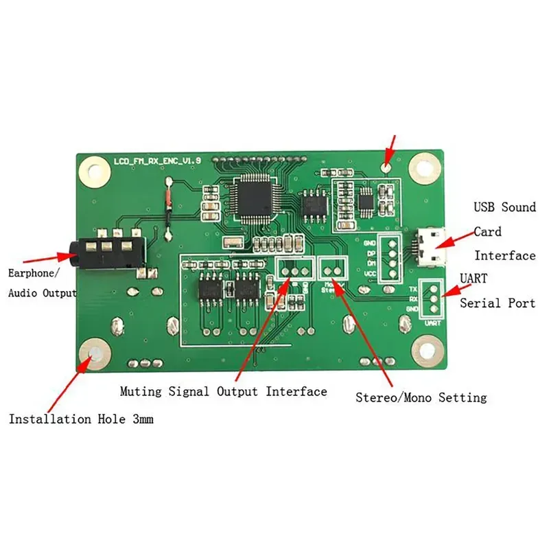
The Critical Role of PCBs in Communication Radio Module Performance

A close-up of a communication radio module PCB board
Communication Radio Module PCB

At the heart of every communication radio module lies the Printed Circuit Board (PCB), the unsung hero ensuring optimal performance, signal integrity, and operational efficiency. It acts as the foundational platform that interconnects all electronic components, facilitating the seamless flow of signals, power, and data. The PCB's design and manufacturing quality directly influence the radio module's ability to transmit and receive signals effectively, making it a critical component for reliable communication. This section explores why the PCB is the cornerstone of communication radio module performance, with a focus on signal integrity, impedance control, and thermal management, crucial aspects in high-frequency applications, and communication module PCB design.

The PCB's primary functions are:

  • Signal Integrity:
    Maintaining the integrity of high-frequency signals is paramount. PCBs are designed to minimize signal loss, reflections, and crosstalk, which can degrade the module's performance.
  • Impedance Control:
    Precise impedance matching is crucial for efficient power transfer and minimizing signal reflections, especially in RF circuits. Controlled impedance ensures that signals travel smoothly without degradation.
  • Thermal Management:
    Radio modules generate heat, and effective thermal management is essential to prevent overheating, which can affect performance and lifespan. PCBs incorporate thermal vias, ground planes, and specialized materials to dissipate heat efficiently.
  • Component Support and Interconnection:
    The PCB provides the physical platform to mount and interconnect all the electronic components, including the transceiver, antenna, power supply, and other supporting circuitry.

In essence, the PCB is not merely a supporting structure but an active participant in the radio module's functionality. A well-designed PCB ensures the module performs as intended, delivering robust and reliable wireless communication.

Overcoming Design Challenges in Communication Radio Module PCBs

Designing printed circuit boards (PCBs) for communication radio modules presents a complex array of challenges, crucial for optimal performance. These challenges, including RF interference, antenna integration, power efficiency, and miniaturization, can significantly impact a module's functionality and reliability. Successfully navigating these hurdles requires specialized expertise and advanced PCB solutions. Zero One Solution excels in mitigating these challenges, providing cutting-edge solutions for communication module PCB design and manufacturing.

  • RF Interference Mitigation
    Radio Frequency (RF) interference is a primary concern, leading to signal degradation and performance issues. Zero One Solution employs strategies like proper grounding, shielding techniques, and careful layout design to minimize interference. We utilize advanced simulation tools to predict and address potential interference issues early in the design phase, ensuring robust performance. Our expertise helps guarantee high-frequency PCB solutions that maintains signal integrity.
  • Antenna Integration
    Integrating antennas directly onto the PCB demands precision. We carefully consider antenna placement, impedance matching, and the surrounding environment to optimize signal transmission and reception. Our engineers use specialized software for antenna simulation and optimization, which is crucial for wireless module prototyping. This ensures that antenna performance aligns with the module's operational frequency and design specifications, leading to improved wireless communication.
  • Power Efficiency Optimization
    Efficient power management is crucial for extending battery life and enhancing overall module performance. Zero One Solution focuses on power plane design, component selection, and thermal management to reduce power consumption. We use low-power components and optimize the PCB layout to minimize signal losses and heat generation, thereby maximizing power efficiency for wireless module PCB design and manufacturing.
  • Miniaturization and Component Placement
    The demand for smaller, more compact communication modules requires innovative PCB design. We excel in high-density interconnect (HDI) PCB design and component placement strategies, which enable the integration of more features into a reduced space. Our team optimizes the component layout to minimize signal paths and ensure ease of assembly, providing advanced solutions for miniaturization in complex RF PCB manufacturing.

By addressing these challenges with a comprehensive approach, Zero One Solution provides high-performance, reliable communication radio module PCBs that meet the stringent requirements of modern wireless applications. Our commitment to excellence ensures that our clients receive innovative and optimized solutions tailored to their specific needs.
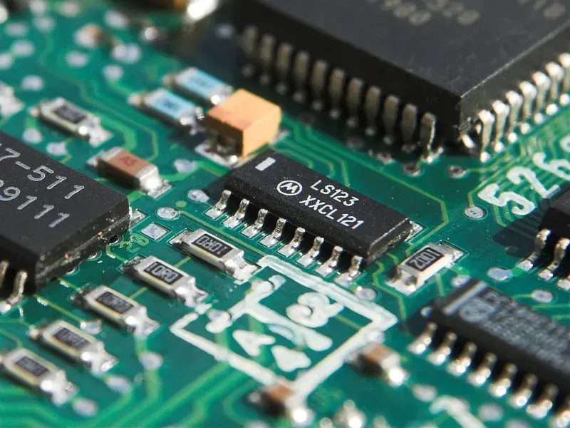
Zero One Solution's Expertise in Communication Radio Module PCB Design

An engineer working on a PCB layout design on a computer screen
PCB Layout Design Engineer

At Zero One Solution, we don't just design PCBs; we engineer solutions tailored to the complex demands of communication radio modules. Our expertise encompasses every facet of PCB design, from the initial schematic capture to the final layout, ensuring optimal performance in high-frequency applications. We specialize in communication module PCB layout and wireless module prototyping, critical steps in RF PCB manufacturing.

  • Schematic Capture and Component Selection
    We meticulously craft schematics, ensuring every component is perfectly selected and positioned for optimal signal integrity and performance. This includes careful consideration of component footprints, placement, and thermal characteristics to mitigate RF interference and ensure reliable operation. Our component selection process prioritizes high-quality, industry-leading components to guarantee long-term reliability and performance in your communication modules.
  • RF-Aware PCB Layout Design
    Our layout design process is optimized for high-frequency applications. We implement controlled impedance traces, minimize signal path lengths, and strategically place components to reduce signal loss and cross-talk. Our engineers utilize advanced simulation tools to validate designs, ensuring they meet stringent RF performance requirements. We specialize in communication module PCB layout, ensuring optimal signal transmission and reception.
  • Expert Antenna Integration
    Integrating antennas directly onto the PCB or in close proximity requires a deep understanding of RF principles. Zero One Solution provides expert antenna integration services, optimizing antenna placement, matching networks, and ground plane designs to maximize antenna efficiency and performance. This is particularly crucial for achieving the desired range and data rates in your communication modules.
  • Power Integrity and Thermal Management
    We pay close attention to power distribution networks to ensure stable power supply to sensitive RF components. Our designs incorporate effective thermal management solutions, such as thermal vias and heat sinks, to dissipate heat generated by power amplifiers and other high-power components. This is vital for maintaining operational stability and extending the lifespan of your communication radio modules.

By leveraging our comprehensive PCB design services, you can accelerate your product development cycle, reduce time-to-market, and ensure your communication radio modules meet the highest standards of performance and reliability. Our proficiency in wireless module prototyping allows us to quickly iterate and validate designs, ensuring your product's success.
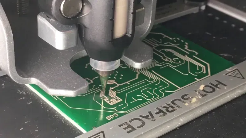
Accelerate Your Radio Module Development with Zero One Solution's Rapid Prototyping

A technician inspecting a freshly prototyped PCB board
Rapid PCB Prototyping

In the fast-paced world of communication radio module development, time is of the essence. Zero One Solution understands this critical need and provides rapid prototyping services that significantly accelerate your product development cycle. Our capabilities enable quick iteration and validation of designs, allowing you to bring innovative solutions to market faster and with greater efficiency.

Our rapid prototyping process includes:

  • Fast Turnaround Times
    We specialize in delivering prototypes within days, not weeks. This speed is crucial for quick design validation and modification.
  • Design Iteration Support
    We provide comprehensive support for design modifications, ensuring that each iteration brings your product closer to perfection. Our engineers are ready to help you fine-tune your communication module PCB layout and other related aspects.
  • High-Quality Manufacturing
    Our prototypes utilize the same high-quality manufacturing processes and materials as our production runs, ensuring reliability and performance.
  • Advanced Technology Integration
    We are adept at integrating advanced technologies, including high-frequency laminates and controlled impedance fabrication, essential for high-performance radio module design.

By choosing Zero One Solution for your rapid prototyping needs, you are not only accelerating your time-to-market but also ensuring the highest quality and performance of your communication radio modules. Our strategic location in Shenzhen, China, and a branch in Dubai, enables us to provide seamless global support for your rapid prototyping requirements. Experience the difference that speed and quality make with Zero One Solution.
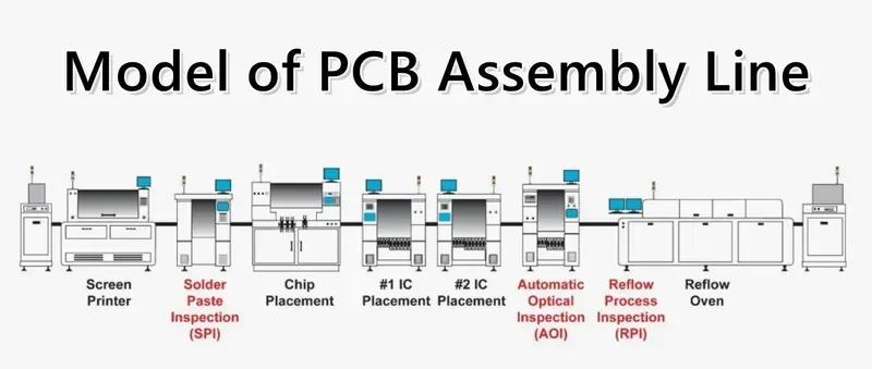
Mastering Advanced PCB Manufacturing for Communication Radio Modules

An automated PCB manufacturing production line with machines
PCB Manufacturing Production Line

The fabrication of communication radio module PCBs demands specialized manufacturing techniques to ensure optimal performance in high-frequency environments. Zero One Solution leverages cutting-edge processes and materials to meet these demands, focusing on high-frequency laminates, controlled impedance fabrication, and precision drilling, thereby providing robust RF PCB manufacturing solutions.

Manufacturing TechniqueDescriptionBenefits
High-Frequency LaminatesUse of materials such as Rogers and Taconic to minimize signal loss and maintain signal integrity at high frequencies.Reduced signal attenuation, improved signal-to-noise ratio, and enhanced overall module performance.
Controlled Impedance FabricationPrecise control of trace width, spacing, and dielectric properties to achieve specific impedance values, such as 50 ohms.Minimizes signal reflections and ensures optimal signal transmission, crucial for RF applications.
Precision Drilling and Via CreationEmploying advanced drilling techniques to create accurate vias, minimizing signal leakage and crosstalk.Improved signal integrity, reduced parasitic effects, and enhanced module reliability.
Surface Finish and PlatingUse of ENIG, immersion silver, or other suitable finishes to provide excellent solderability and prevent corrosion.Ensured reliable solder joints, long-term durability, and optimized RF performance.

These specialized manufacturing processes are critical for high-frequency PCB solutions, enabling us to deliver communication radio module PCBs that meet the stringent requirements of modern wireless applications. At Zero One Solution, we are committed to pushing the boundaries of PCB manufacturing, ensuring that our clients receive the highest quality and most reliable solutions for their communication radio module needs.
Precision Assembly (PCBA) for Communication Modules: Ensuring Peak Performance

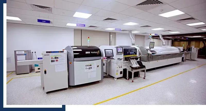
An SMT machine placing components onto a PCB during assembly
PCBA SMT Assembly Machine

Achieving optimal performance in communication radio modules hinges on the precision of the PCB assembly (PCBA) process. Zero One Solution excels in delivering high-quality, reliable PCBA services, crucial for the intricate requirements of RF components and integrated modules. Our advanced Surface Mount Technology (SMT) and through-hole assembly capabilities are specifically tailored to meet the exacting demands of communication radio module PCB assembly, guaranteeing superior product functionality.

Our PCBA services encompass several key aspects:

  • Advanced SMT Assembly
    Employing state-of-the-art SMT equipment, we ensure precise placement of miniature components, essential for high-frequency applications. This precision is critical for maintaining signal integrity and minimizing signal loss in wireless module prototyping.
  • Through-Hole Assembly
    For components that require through-hole mounting, we provide expert soldering services, ensuring robust and reliable connections. This is particularly important for connectors and larger components within the communication radio module.
  • Quality Control and Inspection
    We utilize Automated Optical Inspection (AOI) and X-ray inspection to verify solder joint quality and component placement accuracy. This rigorous quality control process is fundamental to ensuring the dependability of the final product and is essential for communication module PCB assembly.
  • Component Sourcing and Management
    We manage the complete component sourcing process, ensuring that all parts meet the required specifications and are traceable. This includes managing the supply chain for both passive and active components, including the delicate RF components needed for radio modules.
  • Functional Testing
    We perform functional testing to verify that assembled PCBs meet the specified performance criteria. This testing includes signal integrity analysis and RF performance evaluation. This is a crucial step to validate that the communication radio module is functioning correctly after assembly and to ensure that they perform as expected in real-world scenarios.

By focusing on precision, quality, and reliability, Zero One Solution's PCBA services are designed to optimize the performance of your communication radio modules and speed up your wireless module prototyping processes.

The realm of communication radio modules demands precision, expertise, and a rapid turnaround. Zero One Solution Limited stands as your ideal partner, offering a comprehensive, one-stop Communication Radio Module PCB Solution. From initial design consultation and meticulous layout to rapid prototyping and high-volume manufacturing and assembly, we ensure your wireless innovations achieve optimal performance and reach the market swiftly. Leveraging our deep industry knowledge, advanced manufacturing capabilities, and global supply chain network, we transform your concepts into reliable, high-performance communication devices. Partner with Zero One Solution and accelerate your journey from groundbreaking idea to market leadership. Contact us today to discuss your next communication radio module project and experience the Zero One difference.


Anypcba