In an age where personalization reigns supreme, even the humble keyboard has become a canvas for self-expression. The heart of any custom mechanical keyboard lies in its printed circuit board (PCB), the unsung hero connecting switches and electronics. Whether you are a tech enthusiast, a gaming aficionado, or simply a lover of unique tactile experiences, understanding keyboard PCB makers empowers you to craft a keyboard that resonates with your needs and style. This article is designed to guide you through the fascinating world of keyboard PCB creation, from conceptual design to final assembly, giving you the knowledge you need to embark on your custom keyboard journey.
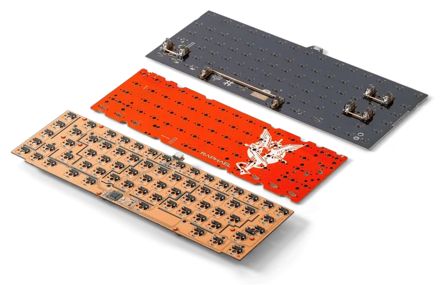
A keyboard Printed Circuit Board (PCB) serves as the foundational platform for all electrical connections within a keyboard. It's a complex structure designed to facilitate communication between the keys, the microcontroller, and ultimately, your computer. Understanding the PCB's components is crucial to designing a custom keyboard or troubleshooting a malfunctioning one.
Key elements of a keyboard PCB include traces, which are conductive pathways that carry electrical signals; vias, which are plated-through holes that connect traces on different layers of the PCB; and switch footprints, the pads where keyboard switches are soldered or installed. Each of these elements plays a crucial role in the overall functionality of the keyboard.
| Component | Function | Description |
|---|---|---|
| Traces | Signal transmission | Conductive paths, typically made of copper, carrying electrical signals between components. |
| Vias | Layer connection | Plated holes connecting traces on different layers of a multi-layer PCB. |
| Switch Footprints | Switch mounting | Pads or mounting points where the keyboard switches are soldered or hot-swapped to the PCB. |
| Microcontroller | Control unit | The 'brain' of the keyboard, processes key presses and communicates with the computer. |
| Diodes | Key matrix | Unidirectional component that prevents ghosting and key rollover issues |
| Connectors | Connectivity | Interface components for USB or other communication connections. |
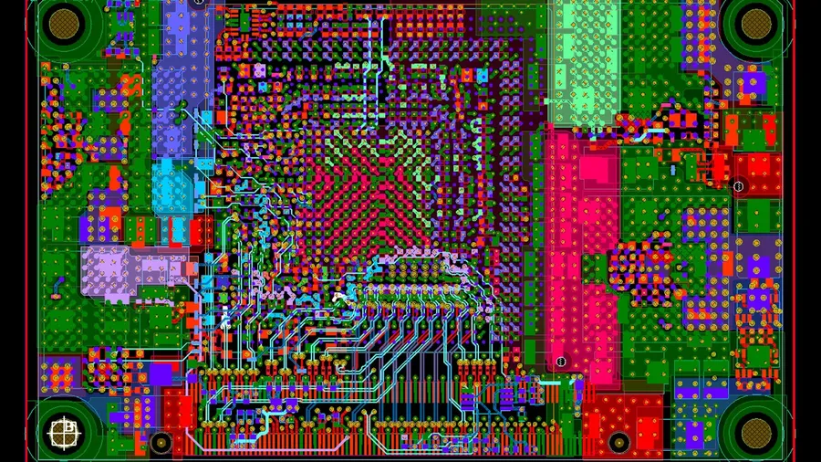
Selecting the appropriate software is crucial for designing a keyboard PCB. The software you choose will significantly impact your design process, capabilities, and the final product. This section explores the landscape of PCB design software, focusing on options suitable for keyboard PCB creation, ranging from free to professional-grade solutions, and considering aspects like learning curve and feature sets.
| Software | Cost | Ease of Use | Key Features | Best For |
|---|---|---|---|---|
| KiCad | Free | Moderate | Open-source, cross-platform, schematic capture, PCB layout, 3D viewer, extensive library. | Enthusiasts and professionals who want a free and powerful option. |
| EasyEDA | Free (with limitations) | Easy | Web-based, easy to learn, schematic capture, PCB layout, integrated library, online collaboration. | Beginners and hobbyists looking for a simple, accessible tool. |
| Eagle (Autodesk) | Subscription-based | Moderate | Industry-standard, powerful, schematic capture, PCB layout, extensive component library, cloud storage. | Intermediate users and professionals who need robust features. |
| Altium Designer | Subscription-based | High | Industry-leading, advanced features, schematic capture, PCB layout, high-speed design, signal integrity analysis. | Professionals working on complex and high-performance PCBs. |
| Fusion 360 (with Electronics) | Subscription-based | Moderate | Integrated CAD and electronics design, cloud-based, collaboration, schematic capture, PCB layout. | Users who need a unified CAD/CAM and electronics design tool. |
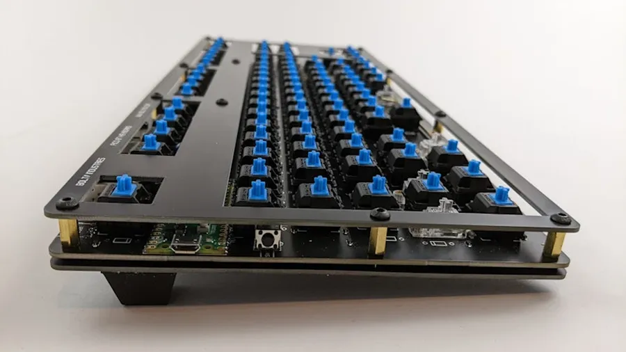
Designing a custom keyboard PCB involves a systematic approach, transforming your concept into a physical circuit board. This process encompasses creating a schematic, selecting appropriate components, meticulously laying out traces, and ensuring both robust grounding and signal integrity for optimal performance. These steps are crucial for creating a functional keyboard.
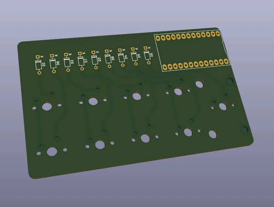
Effective keyboard PCB layout and routing are paramount for achieving optimal performance, reliability, and signal integrity. This section delves into critical aspects such as component placement, trace routing strategies, impedance matching, noise reduction, and minimizing signal interference, providing the necessary information for creating a robust design.
| Consideration | Best Practice | Rationale |
|---|---|---|
| Component Placement | Group related components; place decoupling capacitors near power pins | Reduces signal path length, stabilizes voltage, and minimizes noise. |
| Trace Routing | Minimize length, avoid sharp angles, and use wide traces for power/ground. | Prevents impedance discontinuities, reduces resistance, and enhances signal quality. |
| Impedance Matching | Maintain consistent trace widths, use transmission line techniques, and implement termination resistors | Ensures maximum power transfer, and prevents signal reflections. |
| Noise Reduction | Use effective grounding, ground planes, and decoupling capacitors | Minimizes common-mode noise, reduces crosstalk, and stabilizes power rails. |
| Signal Interference Minimization | Avoid parallel traces, use guard traces, and consider shielding. | Reduces crosstalk and provides isolation for sensitive circuits. |
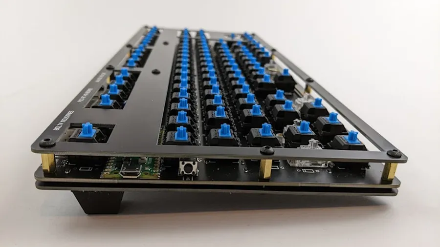
The fabrication of a custom keyboard PCB is a crucial step that bridges your design and a tangible product. This process involves translating your digital design into a physical circuit board, and the selection of manufacturing methods significantly impacts the quality, cost, and timeline of your project. Understanding the various manufacturing options is key to achieving optimal results.
Different PCB manufacturing methods and materials influence the final product and cost, so informed decisions are necessary. It's vital to consider aspects such as fabrication time, volume, material specifications (FR-4 is the standard, but others exist), and surface finish, along with understanding the capabilities of different manufacturers.
| Manufacturing Option | Description | Pros | Cons | Typical Turnaround Time |
|---|---|---|---|---|
| Prototype Services | Specialized for small batch production to validate designs before mass production. | Lower initial cost, suitable for testing and iterations. | Higher per-unit cost, longer lead times for large orders. | 1-2 Weeks |
| Volume Production | Geared towards mass manufacturing for cost efficiency. | Lower per-unit cost, faster production for large batches. | Higher initial setup cost, less flexibility in design changes. | 2-6 Weeks |
| Home PCB Etching | DIY method using chemicals and UV exposure. | Extremely low cost, full design control. | Lower precision, limited complexity, safety concerns. | Variable, often days |
The choice of material significantly impacts the PCB's performance and cost. FR-4 is the most common material, offering a good balance of mechanical strength, electrical insulation, and cost-effectiveness. However, for specialized applications, materials such as high-Tg FR-4, aluminum, or polyimide might be considered. Similarly, surface finishes like HASL, ENIG, or immersion tin affect solderability and corrosion resistance.
Utilizing a professional PCB manufacturer ensures that your PCBs are made with high precision and quality and is often more efficient than DIY methods, which is especially essential for multilayer designs or those with stringent electrical requirements.
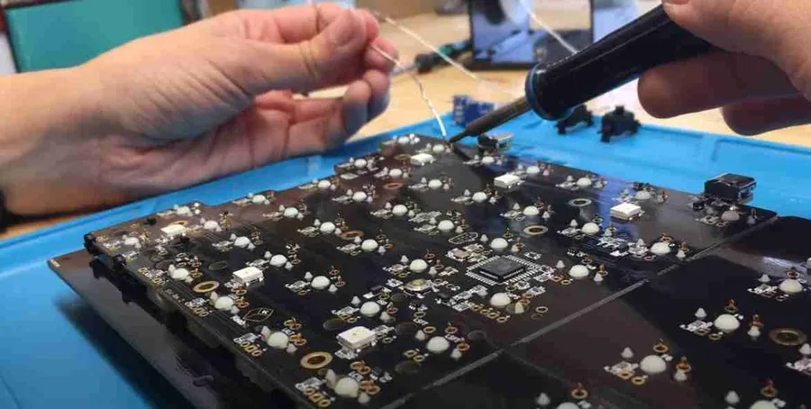
The assembly of a keyboard PCB is a critical step that determines the functionality and user experience of the final product. This section compares and contrasts different assembly methods, focusing on soldering techniques (through-hole and surface mount) and the increasingly popular hot-swap socket approach. Each method has its own set of benefits and drawbacks which will be explored in detail to help inform your decision process.
| Assembly Method | Component Type | Skill Level | Pros | Cons |
|---|---|---|---|---|
| Through-Hole Soldering | Through-hole components | Beginner to Intermediate | Strong mechanical connection; Easier to rework; Visual inspection of solder joints is simple. | Time-consuming; Less compact; Higher profile components; Requires through-hole pads. |
| Surface Mount Soldering (SMT) | Surface mount components | Intermediate to Advanced | Compact; Automated assembly possible; Higher component density. | Difficult to rework; Requires specialized equipment; Small solder joints are harder to inspect visually; Prone to solder bridge issues. |
| Hot-Swap Sockets | Hot-swappable sockets | Beginner | Easy switch replacement; No soldering required; Facilitates experimentation; Damage to PCB from solder heat is eliminated. | Can be less reliable than soldered connections in certain scenarios; Adds cost; Not as secure of a fit as solder. |
Soldering, whether through-hole or surface mount, creates a permanent, reliable electrical connection. Through-hole soldering involves inserting component leads through holes in the PCB and soldering on the opposite side, a more robust connection that is easier to learn but is not space efficient. Surface mount technology (SMT) involves soldering components directly to pads on the surface of the PCB and requires specialized reflow techniques or a steady hand, however SMT allows for increased component density on the board. Hot-swap sockets provide an alternative by creating a mechanical and electrical connection without soldering which makes swapping and changing switches a simple process that doesn't risk damage to the pcb.
The choice between these methods hinges on factors such as the design complexity, the desired level of customization, skill level of the assembler and intended use case. For a single build or prototype hot swap sockets may be more suitable, while those interested in volume production will benefit from the use of SMT and automated assembly.
Troubleshooting a keyboard PCB involves systematically identifying and resolving issues that can arise during design, assembly, or use. These problems can range from simple connection errors to more complex design flaws. Effective troubleshooting requires a logical approach and the use of appropriate tools to isolate the root cause of the problem.
Understanding the most common problems encountered with keyboard PCBs can significantly expedite the troubleshooting process. These issues can be broadly categorized into design flaws, manufacturing defects, assembly errors, and component failures. Proper planning and careful execution are crucial to prevent these issues. This section will equip you with the knowledge to effectively address these problems.
Effective troubleshooting requires a systematic approach. Start by visually inspecting the board for obvious issues like solder bridges, misaligned components or damaged traces. Use a multimeter to check for continuity and shorts, systematically testing each section of the circuit. Diagnostic tools like logic analyzers and oscilloscopes are extremely valuable in analyzing signal integrity and timing issues. Always consult the board's schematic and design documents for reference during troubleshooting. Following these steps will lead to a much more efficient resolution to keyboard PCB problems.
This section addresses common questions about keyboard PCBs, providing concise, authoritative answers to guide you in your custom keyboard journey. These FAQs aim to clarify key concepts, design choices, and practical considerations related to keyboard PCB design and manufacturing.
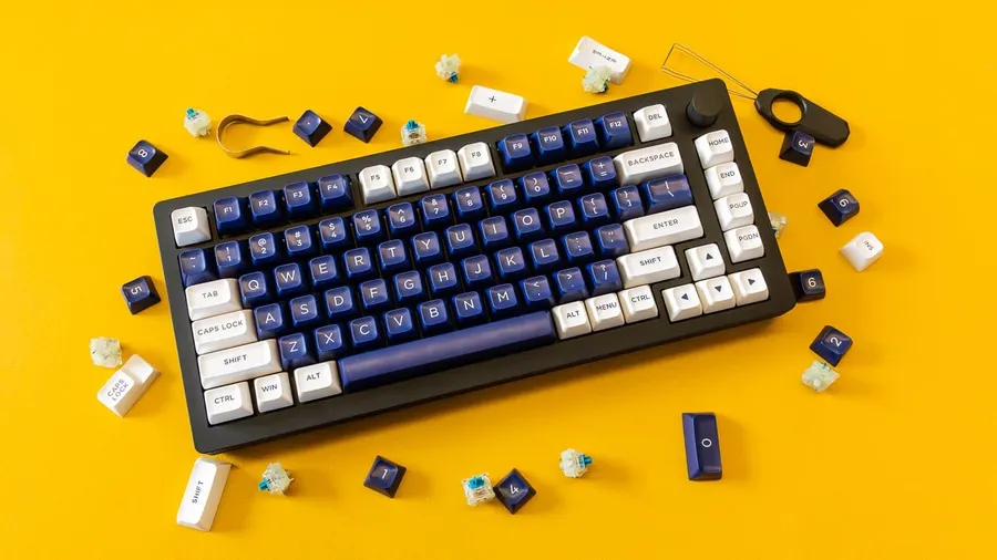
Beyond the fundamentals, keyboard PCB design offers a realm of advanced techniques and customization options to truly personalize your input device. This section explores possibilities such as integrated RGB lighting, custom layouts beyond the standard matrix, alternative component placements for unique aesthetics, and incorporating advanced functionalities for a truly bespoke keyboard.
These advanced features require careful planning and execution. Thorough consideration of design constraints, component selection, and manufacturing capabilities will help realize complex designs.
The journey of crafting a custom keyboard PCB, guided by the knowledge of the keyboard pcb maker, may seem complex at first glance, but with the right tools, knowledge and patient experimentation, it can be a rewarding endeavor. By understanding the key elements of design, production, and assembly, you can create a keyboard that truly matches your needs, style, and preferences. As technology continues to advance, new tools, techniques, and possibilities will become available, making the world of custom keyboard PCBs ever more dynamic and innovative. The future of keyboard technology lies in the hands of those who dare to design.

