Effortlessly Order PCBs with EasyEDA: A Comprehensive Guide
2025.01.08
In today's fast-paced electronics world, turning your circuit designs into physical reality needs to be quick and efficient. EasyEDA, with its integration with JLCPCB, simplifies the PCB ordering process. This guide walks you through every step, from preparing your design to receiving your manufactured boards, offering insights on how to order PCBs, and options for assembly and components, ensuring that turning ideas into tangible electronic devices is easier than ever with the easyeda order pcb process.
Preparing Your PCB Design in EasyEDA for Ordering
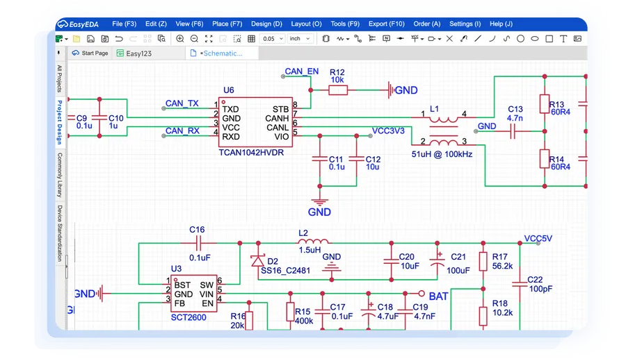
EasyEDA PCB Design
Before initiating an EasyEDA PCB order, a meticulous review of your design is crucial. This involves a thorough verification of your schematic, PCB layout, and all electrical connections, ensuring they are free of errors. A primary focus should be on ensuring all components are sourced from the 'LCSC Assembled' library, facilitating seamless assembly.
Schematic Verification Carefully check for logical errors in your schematic, ensuring component values, pin assignments, and net connections are accurate. Verify that all components are correctly referenced and that no critical components are missing or mislabeled.
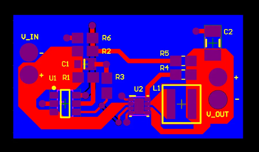
PCB Layout Review Inspect your PCB layout to ensure proper track widths, clearances between traces and pads, and proper component placement. Check for any shorts, opens, or accidental overlaps. Confirm that the chosen trace widths adhere to your current and voltage requirements.
Component Library Usage Ensure all components used in the design are from the 'LCSC Assembled' library to ensure compatibility with JLCPCB's assembly service and accurate BOM generation. Confirm all the part numbers are correct before proceeding.
Design Rule Checks Utilize EasyEDA’s Design Rule Check (DRC) to find any violations of PCB manufacturing standards. Review and resolve all errors and warnings before proceeding with the order.
Generating Gerber Files for PCB Manufacturing
Gerber Files
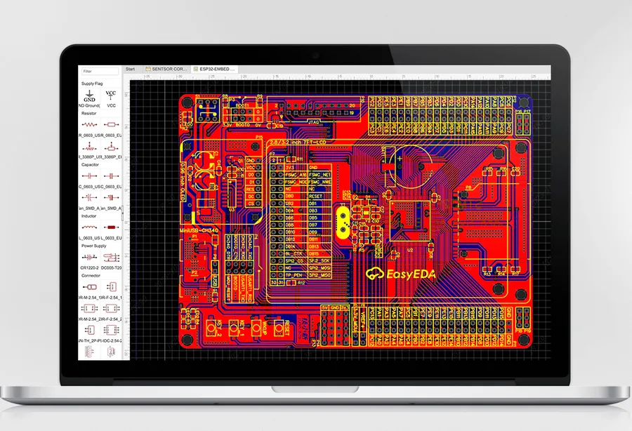
Gerber files are the industry-standard format for communicating PCB design information to manufacturers, enabling the precise fabrication of your electronic circuits. Accurate Gerber file generation is paramount, as these files dictate the final physical characteristics of your board, including layer patterns, drill hole locations, and component placements. EasyEDA simplifies this process, allowing for direct generation of the necessary Gerber files.
Open Your PCB Design Launch EasyEDA and open the specific PCB design project for which you need to generate Gerber files.
Navigate to the Fabrication Output Menu Within the EasyEDA editor, locate the 'Fabrication Output' option usually found in the 'File' menu or a dedicated toolbar.
Select 'Generate Gerber Files' Initiate the Gerber file generation process by clicking on the 'Generate Gerber Files' button or similar. EasyEDA will process your design and compile the required information.
Configure Gerber Settings A dialog window will likely appear, allowing you to customize settings such as units (typically in millimeters or mils), and the specific layers to include. Ensure all necessary layers like copper layers, solder mask, silkscreen, and drill files are selected. It is best practice to keep the default settings unless you have a specific reason to change it.
Review Output Preview If available, review the output preview. This will allow you to verify that all the layers are correctly generated and will help to identify any errors. Ensure the file names are sensible and clear
Download the Gerber Files Finally, download the generated Gerber file package. Typically these files are compressed into a ZIP file. This ZIP file contains all the required files for manufacturing, which will be used in the next step of the process.
Uploading Your Files to JLCPCB for EasyEDA Order PCB
JLCPCB Website
To initiate the PCB manufacturing process, uploading your Gerber files to JLCPCB directly through the EasyEDA interface is essential. This streamlined integration simplifies the transition from design to production. This process involves a series of crucial steps to ensure the correct fabrication of your PCB design, including specifying the necessary parameters to get a quote.
Accessing the JLCPCB Order Interface Within the EasyEDA editor, locate and click on the 'Fabrication Output' button. This will open up the JLCPCB order panel. Ensure you are logged into your JLCPCB account for seamless integration.
Initiating the Gerber Generation Once the order panel is open, EasyEDA will begin generating your Gerber files. This process ensures the files are in the appropriate format for PCB fabrication. This step is automated by EasyEDA.
Specifying PCB Parameters Carefully specify the required PCB parameters. This includes: Material Type (e.g., FR-4), PCB thickness (e.g., 1.6mm), layer count (e.g., 2 layers or 4 layers), copper weight (e.g. 1oz), surface finish (e.g. HASL or ENIG), and other custom specifications that your design demands. Ensure these selections match your design requirements.
Reviewing Design for Assembly (DFA) Verify all parts are using 'LCSC Assembled' class libs. JLCPCB Assembly service requires all parts to be in the LCSC component database with 'basic' or 'extended' options to proceed with SMT Assembly orders.
Confirming Your Order Details Before finalizing the upload, review all entered parameters and the generated Gerber files. Pay special attention to the board dimensions, drill files, and all manufacturing specifications, to avoid errors. Click 'Save to Cart' or 'Order Now' to proceed to checkout. A visual preview is usually available for a final check of your PCB design.
Completing the Order Process Once the design review is complete, proceed to checkout. This includes selecting shipping methods, entering payment information, and confirming the overall cost of your PCB order. JLCPCB will provide you with an estimated delivery time and tracking number after payment is successfully processed.
Understanding PCB Order Pricing and Shipping
PCB Quote
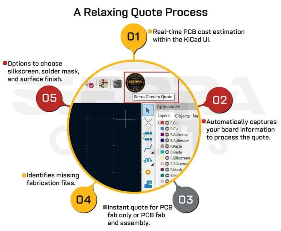
Navigating the costs associated with PCB orders requires a clear understanding of the various factors that influence pricing and shipping. This section provides a breakdown of these elements, offering insights into how board size, order quantity, manufacturing options, and shipping methods impact the total cost of your EasyEDA PCB order.
Cost Factor
Description
Impact on Price
Board Size
The physical dimensions of your PCB.
Larger boards generally cost more due to increased material usage and processing time.
Order Quantity
The number of PCBs you are ordering.
Unit prices typically decrease with larger quantities due to economies of scale.
Layer Count
The number of copper layers in the PCB.
More layers add complexity and increase costs.
Material Type
Specific PCB substrate material (e.g., FR4, aluminum).
Different materials have varying costs based on performance characteristics.
Thickness
The overall thickness of the PCB.
Non-standard thicknesses may incur higher costs.
Finish
The surface finish applied to the PCB (e.g., HASL, ENIG).
More advanced finishes like ENIG can increase cost.
Special manufacturing requirements will increase costs.
Shipping Method
The chosen shipping carrier and speed.
Express options generally cost more but offer faster delivery.
Shipping Distance
The geographical distance between the manufacturer and the delivery address.
Longer distances generally increase shipping costs.
To optimize your PCB order costs, consider these strategies: First, carefully evaluate your design to minimize board size and layers where possible. Second, plan your orders to take advantage of quantity discounts. Third, choose standard materials and finishes unless you have a specific performance requirement. Finally, understand that shipping costs can be a significant component of the total cost, so explore different shipping options and estimated delivery times to find the best balance between cost and speed.
Component Sourcing and Ordering for EasyEDA PCBs
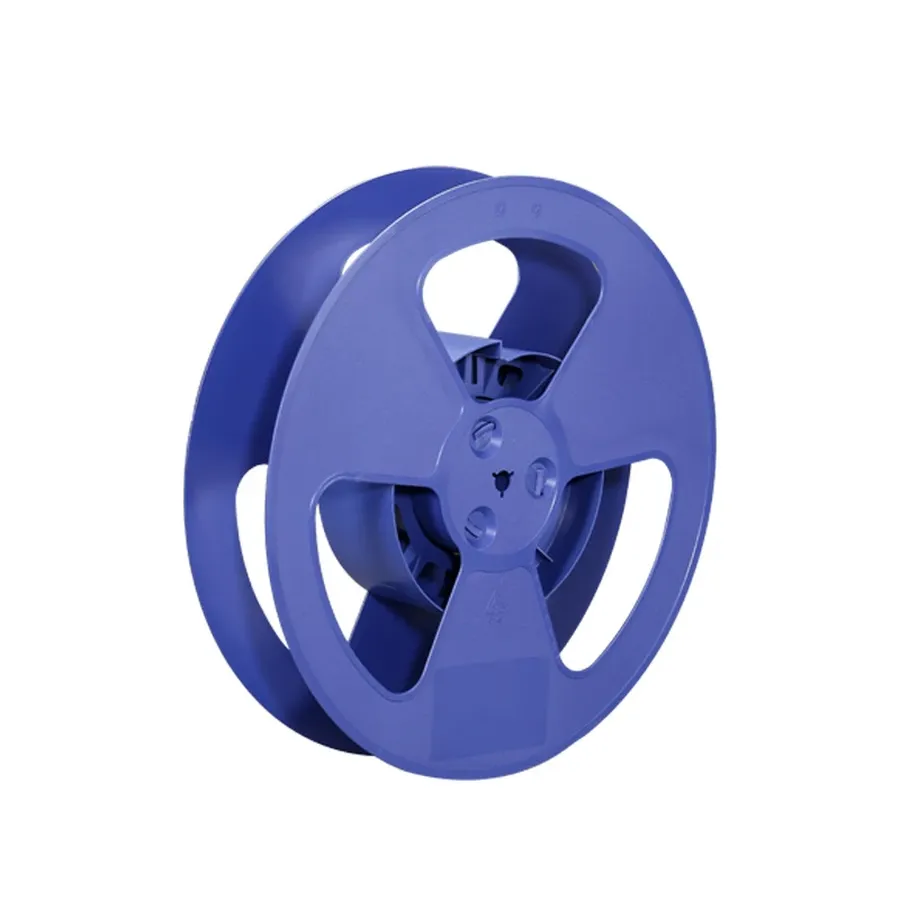
Component Reels
Efficient component sourcing is pivotal for successful PCB assembly. EasyEDA's integration with LCSC streamlines this process, allowing direct access to a vast catalog of electronic components for your PCB projects, which seamlessly integrates with JLCPCB's assembly service.
By ensuring all your parts are of the 'LCSC Assembled' class, you guarantee compatibility with JLCPCB's pick-and-place machines, reducing potential delays and ensuring higher assembly success rates. This integration provides a seamless experience from design to fully assembled PCBs.
Direct Integration with LCSC EasyEDA provides a direct interface to LCSC's component catalog. This allows you to search, select, and add parts directly to your project's Bill of Materials (BOM), streamlining the sourcing process.
Component Selection Choose components that are readily available on LCSC to ensure they are easily procured for assembly. Using 'LCSC Assembled' parts is highly recommended for efficient SMD assembly.
Real-time Stock and Pricing LCSC integration allows you to view the real-time stock levels and pricing of components directly within EasyEDA. This ensures that you select parts that are not only suitable but also readily available and within your budget.
Short Time Ordering Once your design is finalized and the components are selected, you can directly order the components through the EasyEDA interface. This simplifies the sourcing and ordering process, enabling faster assembly of your PCBs.
Feature
Description
Direct BOM integration
Enables seamless part selection and ordering from LCSC.
Real-time inventory information
Displays part availability and pricing directly within EasyEDA.
Reduced order times
Fast component procurement via LCSC.
SMD Assembly Services: Ordering Assembled PCBs
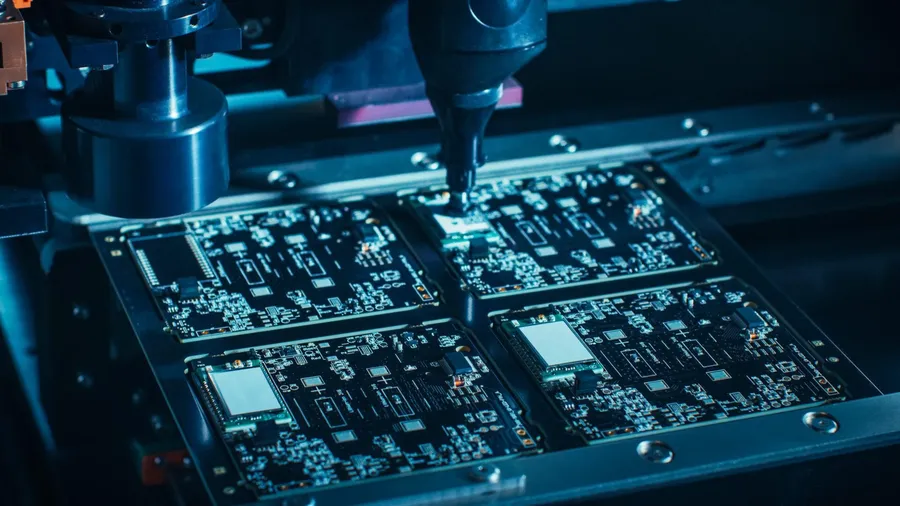
SMT Assembled PCB
Ordering assembled PCBs through EasyEDA and JLCPCB simplifies the electronics manufacturing process by integrating component sourcing and board assembly. This streamlined approach offers a significant advantage over manual assembly, especially for surface-mount devices (SMD), saving time and reducing potential errors. Ordering assembled PCBs involves providing not just the Gerber files, but also a Bill of Materials (BOM) and Pick and Place (PNP) files, which are crucial for automated assembly.
Bill of Materials (BOM) A BOM is a comprehensive list of all the components required for your PCB assembly. It includes the manufacturer's part number, the quantity needed, and the component's designator in the PCB layout. Accurate BOM information is essential for ensuring the correct parts are used during assembly.
Pick and Place (PNP) Files PNP files provide the XY coordinates and rotation information for each component on the PCB. This file is used by automated assembly machines to precisely place components onto the board. Ensure that your design software outputs PNP files correctly, aligning with the board's design origin and using consistent units.
LCSC Component Sourcing LCSC is a direct-to-manufacturer platform for sourcing electronic components, which are integrated with JLCPCB assembly services. When designing your PCB in EasyEDA, select components from the LCSC catalog to ensure their availability and compatibility with the automated assembly process. Using LCSC components streamlines the whole assembly process, as these are readily available at JLCPCB.
The advantages of using surface mount assembly services are considerable. Automated pick-and-place machines improve assembly precision and speed, greatly reducing human error. This approach is highly cost-effective for moderate to high quantities of PCB, as you’re able to streamline the manufacturing process by ordering parts and assembly from the same platform. Additionally, the use of automated assembly helps in managing smaller components, allowing more complex designs to be manufactured efficiently.
Troubleshooting Common PCB Ordering Issues with EasyEDA
Encountering issues during the PCB ordering process in EasyEDA is not uncommon. Understanding how to interpret and resolve these issues, especially warnings and error messages, is crucial for ensuring a smooth and successful manufacturing process. This section provides guidance on identifying, understanding, and rectifying common problems before finalizing your order.
During the order placement, EasyEDA performs several checks to validate your design files and project specifications. These checks are essential for preventing manufacturing errors. Pay close attention to warning messages, as they indicate potential issues that could impact the final product. Error messages, on the other hand, typically halt the order process, requiring you to fix the problem before continuing.
Warning Messages Warnings are not critical issues, but they indicate potential concerns that you should investigate. Examples include small trace widths, vias placed too close together, silkscreen overlapping pads, components not using 'LCSC Assembled' class libraries. Always double check the design file before proceeding.
Error Messages Error messages are critical and will prevent you from placing the order until resolved. Common errors include missing Gerber files, invalid file format, conflicts in board layers, or incorrect component orientation. These usually are related to the design software or the file upload procedure.
File Recognition Errors If the system fails to recognize your files, ensure they are in the correct format (Gerber RS-274X format), are named correctly, and are uploaded to the correct location. Using a zip file can also help with file recognition. Incorrect file formats will lead to parsing errors during the order processing.
Component Placement Issues When ordering assembled PCBs, issues with component placement, such as parts missing from the BOM or pick-and-place files, will cause errors. Double check that components are using 'LCSC Assembled' class libraries, all parts have a unique footprint, the orientation is correct, and the coordinates are precise. Cross-reference data in the BOM and pick-and-place files to ensure consistency.
Design Rule Check (DRC) Errors These errors arise from violating design rules defined by the manufacturing process, such as minimum trace width or clearance. Check and correct your design to pass the DRC before re-generating Gerber files for manufacturing. You may need to adjust your design settings to comply with the rules or adjust the rules based on your needs.
PCB Assembly Frequently Asked Questions About EasyEDA Orders
This section addresses frequently asked questions regarding PCB assembly and ordering through EasyEDA, clarifying common points of confusion and providing concise, authoritative answers to streamline your PCB fabrication process. It covers a range of topics, from basic ordering processes to more complex assembly-related inquiries, designed to equip users with the knowledge necessary for successful project completion.
How do I order a PCB through EasyEDA? To order a PCB via EasyEDA, first complete your PCB design and generate the necessary Gerber files. Then, navigate to the 'Fabrication Output' section of your EasyEDA project, select JLCPCB as your manufacturer, specify your desired PCB parameters (material, thickness, quantity, etc.), and follow the prompts to complete the order. Ensure all components are in the 'LCSC Assembled' class libraries for assembly orders.
What is a PCB order in the context of EasyEDA? A PCB order in the context of EasyEDA refers to the process of sending your designed circuit board data (Gerber files) to a manufacturer, such as JLCPCB, to produce physical PCBs. This encompasses all the steps from design completion in EasyEDA, Gerber file generation, parameter specification, and payment, ultimately resulting in the physical creation of your circuit board.
Can I order a PCB using Gerber files from other design software through EasyEDA? While EasyEDA is primarily designed to streamline the process from design to manufacture, you can upload Gerber files generated from other software when ordering through JLCPCB. However, for optimal integration and ease of ordering, it's generally advised to work within the EasyEDA ecosystem. When using externally generated Gerber files, carefully inspect the uploaded file preview to verify that all layers are correctly imported and the PCB is displayed as intended before proceeding with the order.
How do I order an assembled PCB with components using EasyEDA and JLCPCB? To order assembled PCBs, ensure your design uses components from the LCSC library marked for assembly, and generate a Bill of Materials (BOM) and Pick-and-Place (PnP) files. These files are essential for the assembly service. When ordering, specify the assembly option, and the manufacturing process will include placing components onto the board.
What should I do if I encounter errors during the PCB ordering process in EasyEDA? Errors during the ordering process in EasyEDA commonly involve file issues, component incompatibilities, or incorrect parameter settings. Carefully examine error messages provided by the platform. Common errors might be related to incomplete Gerber files or components not specified for assembly. Address these issues by reviewing your design, ensuring all files are complete, and confirming all parts are in the 'LCSC Assembled' libraries. If problems persist, consult EasyEDA's or JLCPCB's documentation or support.
How can I ensure the best quality for my PCB order through EasyEDA? To ensure the best quality of your PCB, meticulously review your design before submitting your order. Verify that all traces, vias, and pad placements are correct and meet design rule requirements. Select appropriate PCB parameters like material, thickness and surface finish for your project’s specifications. Prior to ordering, thoroughly inspect the previews of your Gerber files, and consider ordering a small quantity prototype to evaluate the quality before large-scale production.
Can I use components outside the LCSC library? EasyEDA is designed for seamless integration with LCSC component library. For assembly service via JLCPCB, it is recommended to use only components from the LCSC library that are marked for assembly. Using components outside this library will require manual sourcing and may not be supported within the automated assembly process of JLCPCB. Therefore, for a smooth assembly process, ensure all components are sourced from the available 'LCSC Assembled' class libs.
Combining Orders and Shipping
Optimizing shipping costs is crucial when ordering PCBs. Combining multiple orders into a single shipment can significantly reduce expenses and streamline your logistics, as well as potentially qualifying for bulk order discounts from the manufacturer. This section details how to leverage combined orders to maximize your savings and efficiency with EasyEDA and JLCPCB.
Order Consolidation Combine your EasyEDA PCB orders into a single shipment. This can be achieved by placing multiple PCB designs within the same order on the JLCPCB platform through EasyEDA, reducing individual shipping fees.
Timing Your Orders Strategically plan your PCB orders so that they can be manufactured and shipped together. This means if you have multiple designs ready, it is more cost-effective to send them as one batch rather than separately.
Shipping Options Familiarize yourself with the shipping options available through JLCPCB. Determine which option best balances cost and delivery time, especially for combined orders that may have a higher weight or volume. Note, it might be more cost effective to select longer delivery time options in bulk orders.
Quantity Discounts Understand how order quantities influence prices. Ordering multiple copies of the same board can reduce the per-unit cost, and in some instances, can also lower the overall shipping costs when combined.
Ordering PCBs with EasyEDA and JLCPCB is a streamlined process that simplifies electronic prototyping and manufacturing. By following the steps outlined, from design to order, including component sourcing and assembly, you can confidently turn your electronic concepts into reality. Remember, understanding the nuances of design preparation, component sourcing from LCSC, and file generation ensures a smooth easyeda order pcb experience. The ability to leverage EasyEDA and JLCPCB will empower you to create innovative electronic projects efficiently.