In today's rapidly evolving tech landscape, custom PCBs (Printed Circuit Boards) are the backbone of countless electronic devices. From powering our smartphones to driving complex industrial machinery, their versatility is unmatched. But the question of 'custom pcb cost' often arises. This article will unravel the complexities of PCB pricing, guiding you through the factors that influence cost, helping you make informed decisions, and ensuring your project stays within budget while maintaining quality. Whether you're an experienced engineer or a budding maker, this guide will equip you with the knowledge to navigate the landscape of custom pcb costs and make more informed decisions when it comes to your next project.
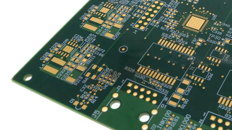
Custom PCB (Printed Circuit Board) costs are influenced by a multitude of factors, each contributing to the overall expense of manufacturing. These factors range from the physical dimensions of the board and its complexity to material choices and order specifics. Understanding these key cost drivers is crucial for effective budgeting and design optimization. This section will delve into the primary factors that dictate the cost of custom PCBs, providing a detailed perspective on each element.
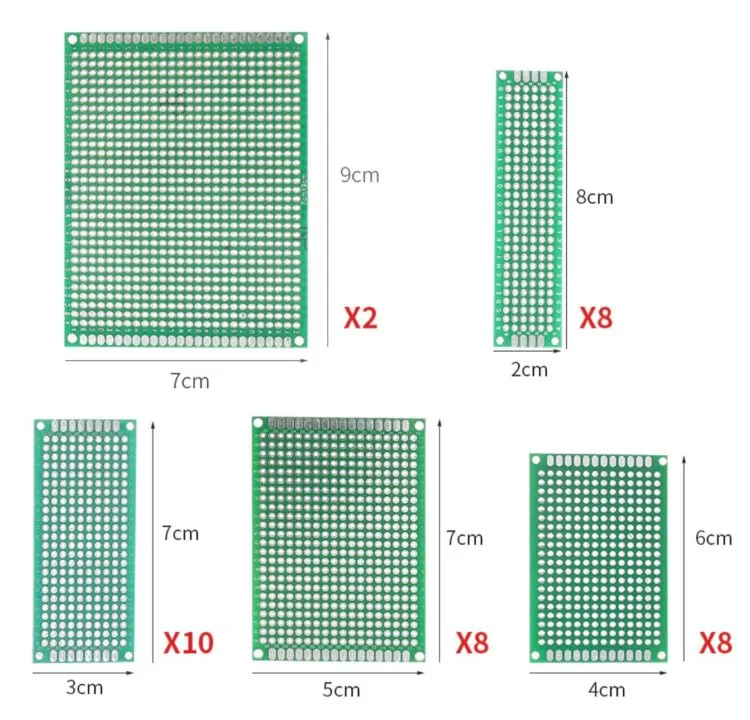
The physical dimensions of a printed circuit board (PCB), along with the number of conductive layers it incorporates, are primary determinants of manufacturing cost. Larger boards and increased layer counts directly translate to higher material consumption and more complex processing, thereby escalating the overall cost.
Specifically, as PCB dimensions increase, more raw material is needed, which increases material costs. In addition, processing time also goes up for larger PCB boards. Moreover, the complexity of manufacturing is greatly increased with the need for more complicated fabrication processes and equipment, further increasing costs.
| Parameter | Impact on Cost | Reasoning |
|---|---|---|
| Increased Board Size | Higher | Greater material usage, extended processing time |
| Increased Layer Count | Higher | More complex lamination, additional processing steps, potentially lower yields |
| 4-layer PCB vs. 2-layer PCB | Higher | Additional layers require more materials, more processing steps and increase fabrication complexity. |
| 8-layer PCB vs. 4-layer PCB | Higher | Additional layers require more materials, more processing steps, increased fabrication complexity and more stringent tolerances. |
The layer count of a PCB refers to the number of conductive layers, each typically made of copper, that are laminated together to form the board. PCBs can range from single-layer (one conductive layer) to multi-layer boards (containing many conductive layers). Multilayer PCBs are typically used for complex designs, but as the number of layers goes up, so does the cost of production. This is due to the more complicated fabrication process, including the additional lamination steps and the increased risk of manufacturing defects, which are harder to resolve in multi-layer PCBs.
In summary, both board size and layer count exert a significant influence on the cost of a PCB. While these parameters may be indispensable in meeting specific design requirements, careful consideration should be given to their impact on the overall budget. It's generally beneficial to strive for the smallest board size and the minimum number of layers that meet the functional requirements.
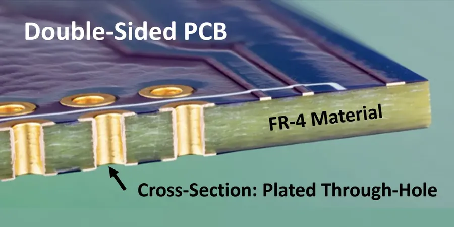
The choice of material for a PCB significantly influences both its cost and performance. While FR-4 is the industry standard, advanced materials offer enhanced electrical, thermal, and mechanical properties but come at a higher price. Understanding these trade-offs is crucial for optimizing your PCB design for its intended application and budget.
| Material Property | FR-4 | Advanced Materials (e.g., High-Speed Laminates, Flexible Substrates) |
|---|---|---|
| Cost | Lower | Higher |
| Dielectric Constant (Dk) | ~4.5 | Variable, often lower for high-speed applications (~3.0 - 3.7) |
| Loss Tangent (Df) | ~0.02 | Lower, typically <0.01, for high-frequency signals |
| Thermal Conductivity | Low | Can be higher, especially with metal-backed boards or specific thermal laminates |
| Maximum Operating Temperature | ~130°C | Can be significantly higher, depending on the specific material |
| Mechanical Flexibility | Rigid | Flexible or rigid-flex options available |
| Application | General-purpose PCBs, low to medium frequency applications | High-speed digital, RF/microwave, flexible circuits, high temperature environments |
The primary consideration when selecting materials is balancing cost with performance requirements. FR-4 offers a cost-effective solution for most general applications, but it may not suffice for high-speed, high-frequency, or high-temperature conditions.
For high-speed applications, materials with lower dielectric constants (Dk) and loss tangents (Df) are essential to reduce signal degradation and maintain signal integrity. For example, materials like Rogers and Isola are frequently used for RF and microwave applications due to their superior electrical properties.
When considering flexible circuits, flexible substrates like polyimide offer the mechanical bendability needed for unique applications. These materials, while more costly than FR-4, provide a solution where rigid PCBs are unsuitable.
The decision to use advanced materials should be carefully evaluated based on the specific requirements of your project. It's crucial to ask if the performance gains justify the increased cost. Factors like signal speed, operating temperature, and mechanical stress should all be considered to make the most appropriate material selection.
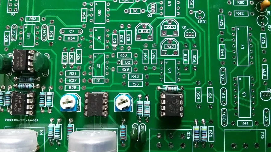
The complexity of a Printed Circuit Board (PCB) design significantly influences its manufacturing cost. Intricate designs necessitate more precise and time-consuming fabrication processes, leading to higher expenses. Features such as fine-pitch components, the density and type of vias, and controlled impedance requirements all contribute to increased manufacturing complexity and, consequently, higher costs.
Several design elements contribute to this increased complexity:
To reduce costs without compromising functionality, consider these design simplification strategies:
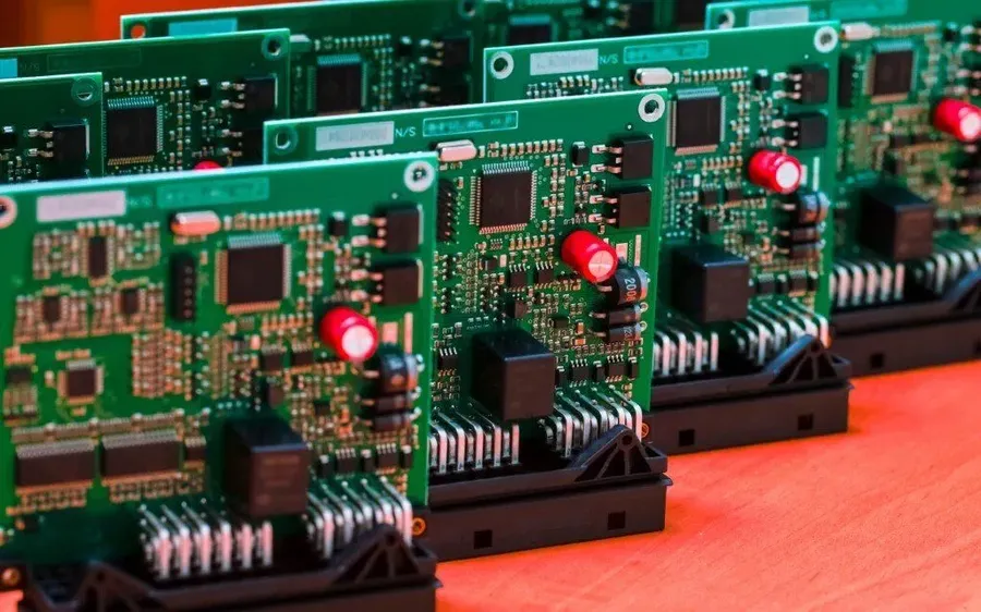
The quantity of PCBs ordered has a profound impact on the per-unit cost, primarily due to economies of scale in manufacturing. Larger production runs distribute fixed setup costs across more units, leading to a significant reduction in the cost per board. This principle is crucial for both prototyping and mass production, and understanding its nuances is essential for effective budgeting.
| Order Quantity | Approximate Per-Unit Cost Impact | Primary Cost Drivers |
|---|---|---|
| Prototype (1-10 units) | High | High setup costs, material waste, manual handling |
| Small Batch (10-100 units) | Medium to High | Reduced setup costs, some automation, material efficiency |
| Medium Batch (100-1000 units) | Medium | Optimized setup, improved material usage, semi-automated process |
| Large Batch (1000+ units) | Low | Highly automated production, minimal setup cost per unit, volume discounts |
Minimum Order Quantities (MOQs) are a critical factor when assessing cost. Most manufacturers enforce MOQs to cover their operational costs. For prototypes or small projects, these MOQs can lead to inflated costs because you might be paying for more boards than you initially need. Therefore, understanding the manufacturer's MOQs early in the design process is essential to optimize cost.
The relationship between order quantity and cost is not always linear. While per-unit costs typically decrease with increasing volume, there can be breakpoints where significant price drops occur due to increased automation and bulk material purchase options. Identifying these breakpoints can help strategically plan production runs to maximize cost efficiency.
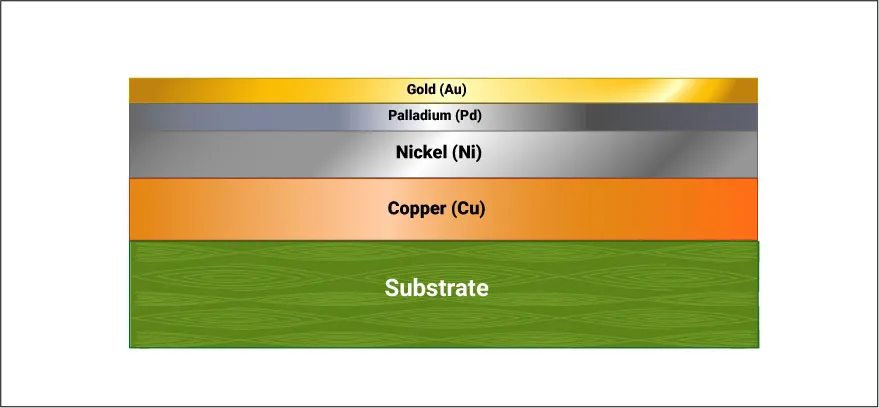
The selection of surface finish and solder mask is a crucial step in PCB manufacturing, directly impacting both the performance and cost of the final product. These choices must align with the intended application and performance requirements, while also considering budgetary constraints. Surface finish affects solderability and long-term reliability, whereas solder mask provides insulation and protection against oxidation.
| Surface Finish | Description | Cost | Pros | Cons | Typical Applications |
|---|---|---|---|---|---|
| HASL (Hot Air Solder Leveling) | Molten solder is applied to the PCB and leveled with hot air. | Low | Low cost, good solderability, widely available. | Uneven surface, not suitable for fine-pitch components, contains lead (lead-free options available but more expensive). | General purpose PCBs, through-hole components. |
| ENIG (Electroless Nickel Immersion Gold) | A layer of nickel is deposited, followed by a thin layer of gold. | High | Excellent solderability, flat surface, good for fine-pitch components, good oxidation resistance. | High cost, can suffer from 'black pad' issues if not manufactured correctly | Fine-pitch components, wire bonding, demanding applications. |
| Immersion Tin | A thin layer of tin is chemically deposited onto the copper pads. | Medium | Good solderability, flat surface, lead-free. | Can be prone to whiskering, requires careful handling. | Lead-free assemblies, general-purpose electronics. |
| Immersion Silver | A thin layer of silver is chemically deposited onto the copper pads. | Medium | Good solderability, flat surface, lead-free, good conductivity. | Susceptible to tarnish, requires special packaging and handling. | High frequency applications, wire bonding. |
| OSP (Organic Solderability Preservative) | A thin layer of organic compound is applied to protect copper before soldering. | Low | Low cost, good solderability, lead-free. | Short shelf life, sensitive to handling. | General-purpose PCBs, SMT assemblies. |
Solder mask is an insulating layer applied to the PCB, except for the solder pads, preventing solder bridges and oxidation. While green is the standard color due to historical reasons, other colors like red, blue, black, and white are available at a slightly increased cost. The choice of solder mask color depends on aesthetic preferences, contrast requirements for silkscreening, and visibility for inspection.
The optimal surface finish and solder mask selection requires a careful evaluation of cost versus performance. For less demanding applications, cost-effective solutions like HASL and standard green solder masks are often sufficient. However, for high-reliability, fine-pitch, or high-performance applications, investing in ENIG or other premium surface finishes may be necessary to ensure the desired product quality and longevity.
Expedited manufacturing and quick turnaround times for custom PCBs significantly impact overall cost, often demanding a premium for faster delivery. Balancing urgency with budget requires careful consideration of the trade-offs between standard lead times and express manufacturing options. Understanding these cost implications is crucial for effective project management and budget adherence.
Standard PCB manufacturing timelines typically range from a few days to a few weeks, depending on the manufacturer and the complexity of the design. Opting for faster turnaround, commonly referred to as a 'rush order,' will incur additional costs due to the manufacturer needing to prioritize your order, reallocate resources, and often pay overtime to production staff. The premium for rush orders can vary greatly, depending on the manufacturer and the urgency of the turnaround requested.
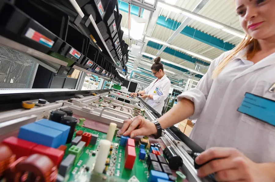
Selecting the appropriate PCB manufacturer is critical for balancing cost, quality, and project requirements. The decision significantly impacts the final product's performance, reliability, and overall budget. A thorough evaluation of different manufacturing options ensures the chosen partner aligns with specific needs and constraints.
There is a wide range of manufacturers, each with unique strengths and focus areas, requiring designers to carefully assess their individual needs against the capabilities of these manufacturers. Factors such as production scale, specific technologies, quality standards, and cost-effectiveness must all be considered.
Here are some key insights and suggestions to consider when selecting a PCB manufacturer:
Understanding the costs associated with custom PCBs can be complex. This section addresses frequently asked questions to provide clarity on the factors influencing PCB pricing.
Understanding the factors that influence custom pcb cost is crucial for planning your electronic projects effectively. By carefully considering board size, layer count, material selection, design complexity, and order quantity, you can significantly optimize your expenses. Whether you're seeking a cost-effective prototype or a large production run, having a firm grasp of these principles will empower you to make informed decisions. As technology advances, it’s important to remain updated on manufacturing process and material developments that can further impact custom pcb costs. With this in mind, continuous learning about PCB design and manufacturing will help to maximize your budget while keeping up with the industry's needs.

