In our increasingly interconnected world, printed circuit boards (PCBs) form the backbone of nearly every electronic device. Among these, the PCB 2, or 2-layer PCB, stands out for its versatility and cost-effectiveness. This article delves into the intricacies of 2-layer PCBs, exploring their structure, design considerations, and applications, bridging the gap between technical complexity and everyday utility, and showing why they are still a mainstay of modern electronics.
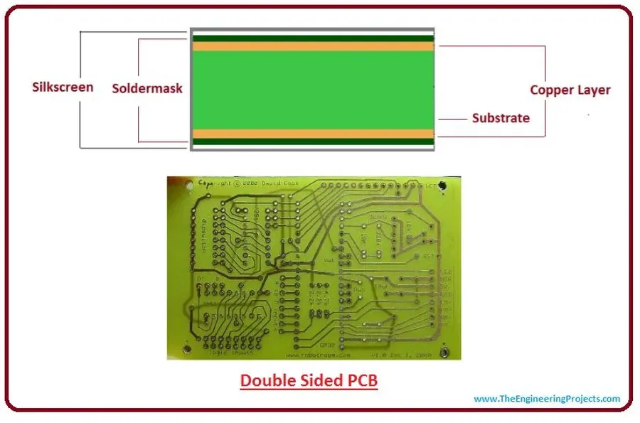
A 2-layer PCB, commonly known as a double-sided PCB, is a printed circuit board characterized by two conductive layers of copper, one on the top surface and another on the bottom, separated by a non-conductive substrate. This configuration enables the creation of relatively intricate electronic circuits while maintaining cost-effectiveness, making it a widely used choice in electronics manufacturing.
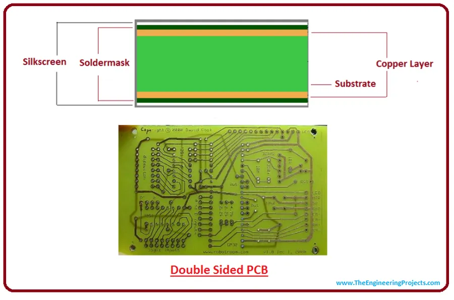
A 2-layer PCB's functionality is defined by its core components: the substrate, copper layers, vias, and solder mask. These components interact to form the structural and electrical basis of the circuit board, allowing for signal transmission and component mounting. Each element plays a crucial role in the overall performance and reliability of the PCB.
| Component | Description | Function | Common Material |
|---|---|---|---|
| Substrate | The base material providing structural integrity. | Provides physical support, electrical insulation between layers. | FR4 (Flame Retardant 4) |
| Copper Layers | Thin sheets of copper adhered to the substrate. | Conducts electrical signals and power. | Electrolytic Copper |
| Vias | Plated holes connecting top and bottom copper layers. | Enables electrical connections between layers. | Copper-plated through-hole |
| Solder Mask | A protective layer applied over the copper. | Prevents solder bridges and protects copper traces. | Epoxy or Liquid Photoimageable (LPI) Solder Mask |
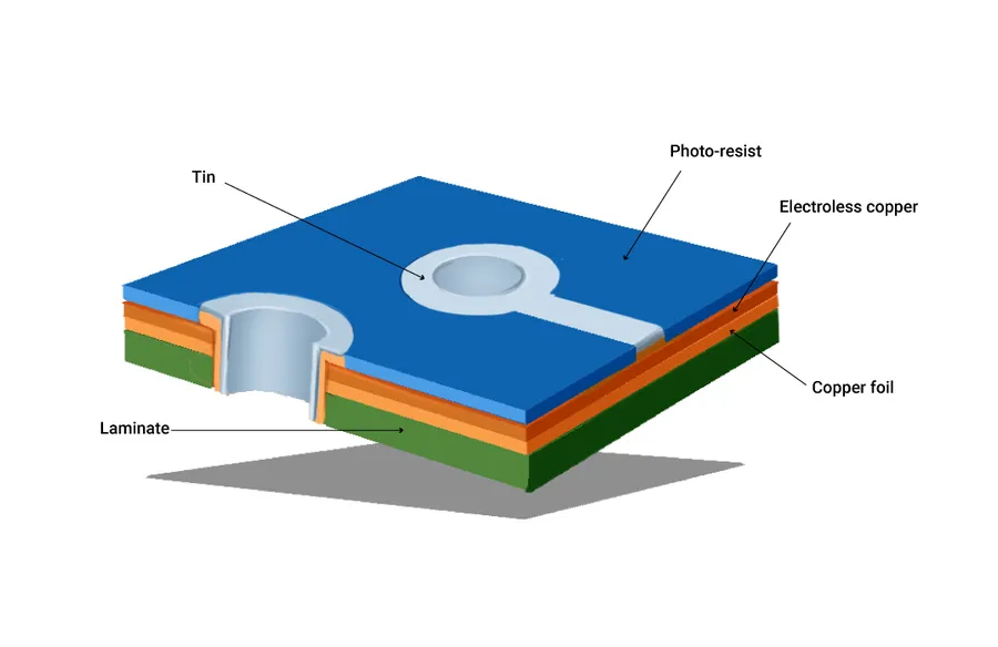
The manufacturing of a 2-layer PCB involves a series of precise steps, each critical to the final functionality and reliability of the board. This process transforms a digital design into a physical circuit capable of performing its intended purpose. Key stages include schematic creation, copper etching, via drilling, solder mask application, and silkscreen printing.
| Manufacturing Step | Purpose | Key Considerations |
|---|---|---|
| Schematic & Layout | Defines the circuit and arrangement of components and traces | Component placement, trace widths, signal integrity |
| Copper Etching | Creates conductive paths on the board | Etch precision, trace dimensions, impedance control |
| Via Drilling | Enables electrical connection between layers | Via diameter, plating quality, reliability |
| Solder Masking | Prevents solder bridges and protects traces | Proper alignment, material type, coverage |
| Silkscreen Printing | Adds component markings, and other references | Clarity, readability, position accuracy |
2-layer PCBs, characterized by conductive copper layers on both sides of an insulating substrate, offer distinct advantages, notably in cost-effectiveness and simplicity. These attributes make them a foundational choice for numerous electronic applications, especially where complexity is not paramount.
| Feature | 2-Layer PCB | Multilayer PCB |
|---|---|---|
| Cost | Lower | Higher |
| Design Complexity | Simpler | More Complex |
| Manufacturing Time | Shorter | Longer |
| Signal Density | Lower | Higher |
| Prototyping Speed | Faster | Slower |
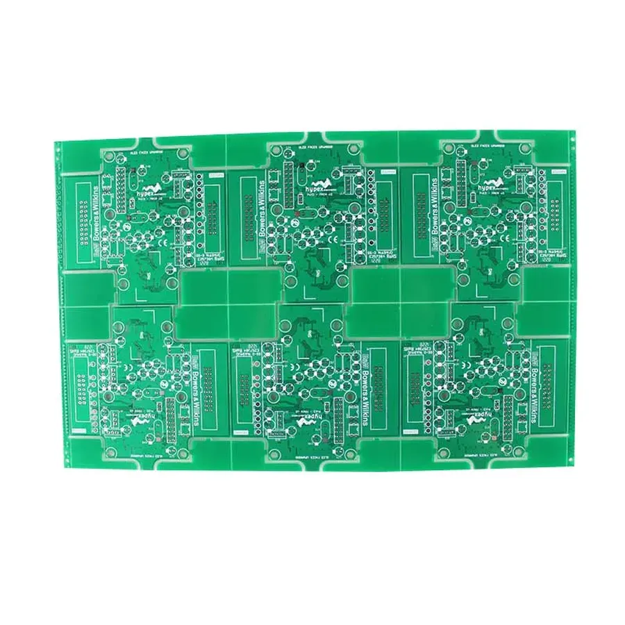
2-layer PCBs, owing to their balance of cost-effectiveness and design simplicity, are integral to a diverse range of electronic applications. Their versatility allows them to be employed in both basic consumer devices and more complex industrial control systems.
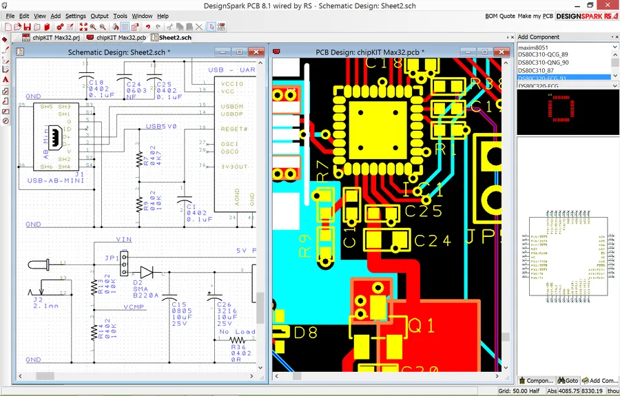
Effective design of 2-layer PCBs requires careful attention to several interconnected factors. These considerations are paramount to ensure the manufactured board operates reliably, avoids signal integrity issues, and fulfills its intended function. Key aspects involve trace geometry, layer stack-up, via implementation, thermal considerations, and adherence to established design guidelines.
| Design Parameter | Description | Impact | Design Rule Best Practices |
|---|---|---|---|
| Trace Width and Spacing | Width and spacing of copper traces on the board. | Affects current carrying capacity, impedance, and crosstalk. | Use appropriate width for current needs and maintain adequate spacing between traces |
| Layer Stack-up | The arrangement of the substrate and copper layers. | Determines impedance control and signal routing. | Select proper layer order to achieve controlled impedance. |
| Via Placement | The location of vias (holes that connect layers). | Impacts signal routing and can cause signal integrity problems. | Place vias strategically and minimize their number |
| Thermal Management | How heat is dissipated by components on the board. | Critical for board longevity and performance. | Provide adequate copper area around heat-generating components. |
| Design Rules & Best Practices | Established guidelines for PCB design. | Ensures reliable manufacturing and function. | Adhere to industry standards and manufacturer recommendations. |
| Layout Planning | The physical organization of components and routing. | Prevents interference and crosstalk. | Strategically position components to minimize signal interference. |
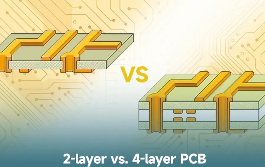
The selection between a 2-layer PCB and a multilayer PCB is a critical decision in electronic design, dictated by the complexity and performance needs of the project. While 2-layer PCBs excel in cost-effectiveness and simplicity, multilayer PCBs offer enhanced density and signal integrity required for more sophisticated applications.
| Feature | 2-Layer PCB | Multilayer PCB |
|---|---|---|
| Complexity | Suitable for simpler designs | Handles complex designs |
| Density | Lower component density | Higher component density |
| Signal Integrity | More susceptible to noise and interference | Better signal integrity due to internal layers |
| Cost | Lower manufacturing cost | Higher manufacturing cost |
| Layer Count | Fixed at two conductive layers | More than two conductive layers |
| Design Time | Faster and simpler design process | Longer and more complex design process |
| Applications | Suitable for basic electronics and low-speed circuits | Suitable for high-speed, high-density, and complex circuits |
The key differentiation lies in the number of conductive layers, with multilayer PCBs utilizing three or more layers. This increased layer count enables designers to route more signals, accommodate higher component densities, and achieve better impedance control, critical for high-speed applications.
Ultimately, the choice depends on a careful evaluation of project requirements, balancing performance needs, cost constraints, and design complexity. If a straightforward circuit design is needed without high density needs or complex signal requirements, then a 2-layer board is sufficient, but if more complex needs exist, then a multilayer is necessary.
This section addresses common questions regarding 2-layer printed circuit boards (PCBs), providing clear and concise answers to assist in your understanding and application of this technology. These FAQs are designed to cover key aspects from basic definitions to design considerations.
The cost of 2-layer PCBs is influenced by several factors, including material selection, board size, complexity of the design, production volume, and the chosen manufacturer. Balancing these factors is essential to achieve a cost-effective solution without compromising quality and desired lead times.
| Cost Factor | Description | Impact on Cost |
|---|---|---|
| Material | Type of substrate (e.g., FR4, CEM-1), copper thickness | Higher-grade materials or thicker copper increase cost |
| Board Size | Physical dimensions of the PCB | Larger boards require more material and processing, thus higher cost |
| Design Complexity | Number of vias, trace density, and board outline shape | More complex designs increase fabrication time and cost |
| Production Volume | Number of PCBs to be manufactured in a single batch | Higher volumes typically result in a lower per-unit cost due to economies of scale |
| Manufacturer Location | Labor costs, facility overheads, and shipping costs | Manufacturers in certain regions might offer lower prices, but this could affect lead times or quality |
| Surface Finish | Type of coating applied to the copper pads (e.g., HASL, ENIG) | Certain finishes provide enhanced performance or corrosion resistance but may add cost |
Sourcing the right PCB manufacturer is as important as design considerations. Consider the following:
PCB 2, the 2-layer PCB, remains a fundamental element in the electronics industry due to its balance of simplicity, cost-effectiveness, and reliability. Understanding their design, fabrication, and applications enables both seasoned and novice engineers to create efficient and robust electronic systems. By considering all factors, PCB 2 can serve as the foundation for diverse electronic devices. This guide provides a roadmap for successfully implementing 2-layer PCBs in your next project and emphasizes their continued importance in modern electronics.

