In today's rapidly advancing technological landscape, Printed Circuit Boards (PCBs) are the unsung heroes powering our devices. From the simplest gadgets to sophisticated medical equipment, PCBs are integral to electronic functionality. Understanding the often-opaque world of PCB design cost is essential for anyone looking to develop electronic products. This article will illuminate the key factors determining PCB design expenses, enabling you to make informed decisions and manage your project budget effectively. By exploring these costs, we aim to demystify the process, akin to understanding the mechanics behind a watch, making the complex world of PCB design accessible to all.

The hourly rates for PCB (Printed Circuit Board) designers exhibit a wide spectrum, ranging from $25 to over $300. This variance is primarily attributed to factors such as the designer's experience level, geographic location, and the intricacy of the specific PCB design project. Understanding these contributing factors is crucial for effectively budgeting and selecting the appropriate design expertise.
| Experience Level | Typical Hourly Rate Range | Project Complexity Impact |
|---|---|---|
| Entry-Level Designer | $25 - $75 | Suitable for simple, standard PCB designs. |
| Mid-Level Designer | $75 - $150 | Capable of handling moderately complex, multi-layer designs. |
| Expert/Senior Designer | $150 - $300+ | Specialized in highly complex, high-density, or high-speed designs. |
When considering hourly rates, it is essential to understand that geographical location significantly impacts costs; designers in metropolitan areas or regions with higher cost of living often command higher rates. The project's complexity is another key driver of cost as more intricate designs involving multiple layers, dense component placement, and high-speed routing require greater expertise and time.
Project-based pricing for PCB design offers a distinct approach compared to hourly rates, where a fixed fee is agreed upon before the work commences. This model is especially favored for projects with well-defined specifications and scope, providing both the client and designer a predictable cost structure, but often requires a detailed up-front analysis.
Typical project-based costs for PCB design can vary significantly, generally ranging from $1,500 to $10,000+, or even more for highly complex designs. These costs are influenced by several factors which are detailed below.
| Cost Factor | Description | Typical Cost Range Influence |
|---|---|---|
| Project Complexity | The intricate nature of the PCB, including the number of layers, component density, and routing difficulty. | Low to high impact |
| Scope of Work | The breadth and depth of the design task, from simple layout to full-scale design with prototyping. | Low to high impact |
| Technology Requirements | Specific technology needs, such as high-speed design, impedance control, or RF design. | Medium to high impact |
| Turnaround Time | The project timeline required, with expedited timelines often incurring higher costs. | Medium impact |
| Designer Expertise | The experience and skill level of the design engineer. | Medium to high impact |
Project-based pricing has its own advantages and disadvantages. One advantage is that it provides cost certainty. Clients know the full cost upfront and thus can budget effectively. This cost clarity can be beneficial for projects with well-defined parameters, and reduces the risk of unexpected expenses due to prolonged design hours. A disadvantage of this pricing method is that it can sometimes lead to higher upfront costs for the client, as designers may incorporate buffers to cover potential challenges or scope changes, which may not materialize. This pricing model is also less flexible when changes to the project scope occur mid-project and can result in additional fees for amendments.
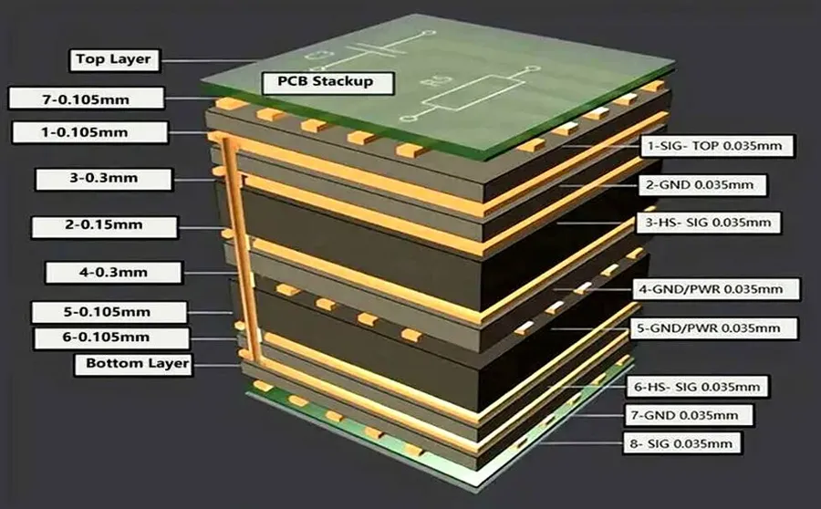
The cost of PCB design is not a fixed figure; it's a dynamic value influenced by a multitude of factors. Understanding these elements is crucial for accurate budgeting and effective project management. These factors span the technical complexity of the board, the resources required, and the expertise involved.
| Factor | Description | Cost Impact |
|---|---|---|
| Board Complexity (Layers) | Number of layers (single, double, multi-layer) | Higher layer count increases cost due to manufacturing complexity and routing challenges. |
| Component Density | Number of components per unit area | Higher density often implies more intricate routing and increased design time, raising costs. |
| Routing Difficulty | Complexity of signal paths and impedance matching | Difficult routing requires more time and specialized expertise, increasing design costs. |
| Software Used | Choice of PCB design software (e.g., Altium, KiCad) | Specialized software licenses, such as Altium, can significantly affect cost due to subscription costs, while open source software like KiCad is free but may have a learning curve. |
| Turnaround Time | Project completion timeframe | Expedited delivery or faster turnaround time usually incurs a higher fee due to resource prioritization. |
| Designer's Expertise | Experience and skill level of the PCB designer | Highly experienced designers with specialized skills command higher rates but often deliver higher quality and more efficient designs. |
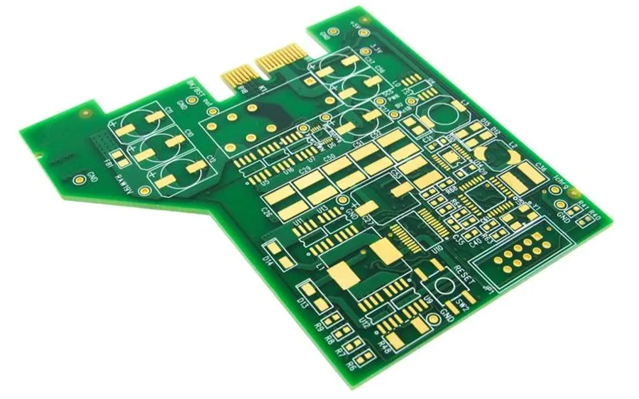
The complexity of a Printed Circuit Board (PCB) is a primary determinant of its design cost, with a direct correlation between the number of layers and overall expense. This section will delve into how the cost of PCB design scales with complexity, comparing simple 2-layer boards to more intricate multi-layer designs.
| PCB Complexity | Typical Cost per Square Inch (Design) | Typical Cost per Square Inch (Manufacturing) | Design Time |
|---|---|---|---|
| Simple 2-Layer Board | $0.50 - $2.00 | $0.10 - $0.50 | Low |
| 4-Layer Board | $1.00 - $3.50 | $0.20 - $0.75 | Medium |
| 6-Layer Board | $2.00 - $5.00 | $0.40 - $1.00 | Medium to High |
| 8+ Layer Board | $3.50 - $10.00+ | $0.80 - $2.00+ | High |
The cost per square inch is a common metric, but it's crucial to note that the overall project cost is also affected by the complexity of routing, component density, and other factors, not just the number of layers. More complex designs require more time for layout and verification, resulting in higher labor costs. The design costs also directly influence the manufacturing costs due to the increased material consumption and processing requirements for multilayer PCBs.
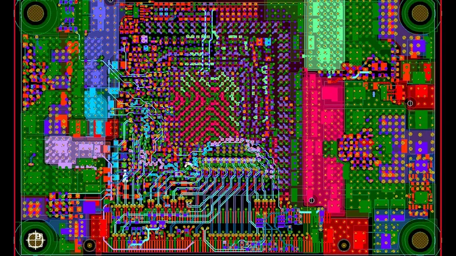
The choice of PCB design software significantly influences the overall project cost. Different software packages have varying licensing fees, learning curves, and capabilities, all of which contribute to the final expense of PCB design.
Professional-grade software often requires substantial upfront investment, whereas open-source alternatives offer cost-effective solutions, yet might require more manual work. The selection process should balance cost, required features, and the designer’s proficiency with the specific software.
| Software | Licensing Cost | Complexity | Expertise Level | Impact on Cost |
|---|---|---|---|---|
| Altium Designer | High (Subscription Model) | High | Expert | High. Contributes to higher design costs due to licensing and specialized skills required. |
| Cadence Allegro | High (Perpetual or Subscription) | High | Expert | High. Known for its advanced features and high cost. |
| KiCad | Free (Open Source) | Medium | Beginner to Intermediate | Low. Can significantly reduce overall design costs due to no licensing fees. |
| Eagle (Autodesk) | Subscription based with free for hobbyist | Medium | Intermediate | Medium. Can be more cost-effective than high-end software, but can increase costs depending on use case |
| OrCAD | High (Subscription) | High | Expert | High. Comprehensive solution that requires significant investment. |
The selection of software often involves a trade-off between cost and capabilities, impacting the total PCB design budget. Furthermore, the expertise required to use these tools will affect labor costs. For instance, a highly skilled designer proficient in Altium may command a higher hourly rate compared to one using KiCad.
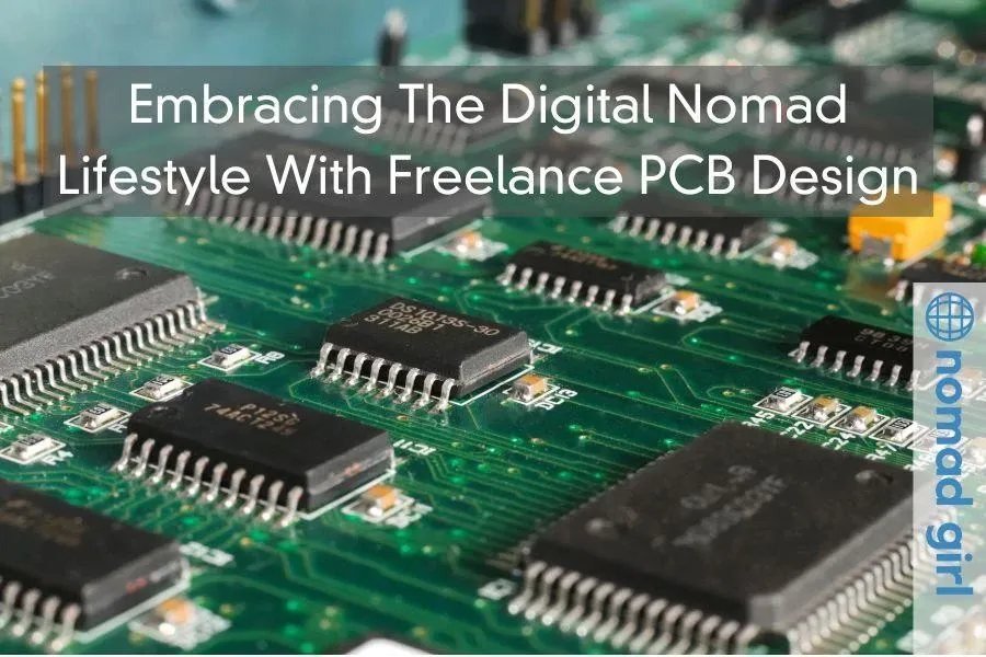
The decision between hiring a freelance PCB designer and engaging a professional design service or firm significantly impacts project cost and outcome. Each option presents distinct advantages and disadvantages, making the choice dependent on specific project needs, budget constraints, and desired level of support.
| Feature | Freelance PCB Designer | Professional PCB Design Service/Firm |
|---|---|---|
| Cost | Generally lower hourly rates; project costs can be more unpredictable. | Higher hourly rates, but often offer fixed project costs; greater cost predictability. |
| Expertise | Expertise varies widely; requires thorough vetting and validation of skills. | Typically has a team of specialized engineers with diverse expertise; quality assurance processes in place. |
| Project Management | Less structured project management; may require more client oversight. | Structured project management; clearly defined processes and timelines; dedicated project manager. |
| Scalability | Limited scalability; difficult to handle large or complex projects. | Highly scalable; capable of handling projects of varying sizes and complexities. |
| Communication | Direct communication with the designer; potential for communication bottlenecks. | Communication managed through a project lead or client manager; clear reporting structure. |
| Turnaround Time | Can fluctuate based on the designer’s availability and workload; potential delays. | Typically adheres to a strict timeline; ability to dedicate resources to meet deadlines. |
| Resources and Software | May have limited access to expensive software and tools; reliance on personal setups. | Access to the latest software and design tools; standardized and well-maintained design environments. |
| Support and Liability | Limited formal support; individual liability. | Offers robust support and warranty; corporate liability. |
Choosing between a freelance designer and a professional service involves a trade-off between cost, scope, and risk. Freelance designers are often suitable for small to medium projects with well-defined specifications and limited complexity, where cost is a primary consideration and the risks are acceptable. Professional services are better equipped to manage larger, more intricate designs requiring multiple design disciplines, offering greater resource capacity and assurance in delivering quality design within established timeframes.
Understanding the costs associated with PCB design is crucial for effective project planning. Here are some of the most frequently asked questions to help clarify the financial aspects of PCB design.
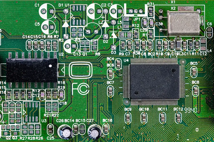
Reducing PCB design costs involves a multifaceted approach, encompassing design choices, process optimization, and strategic vendor selection. By focusing on key areas, significant cost savings can be achieved without compromising quality or functionality. This section details actionable strategies for minimizing expenses associated with PCB design.
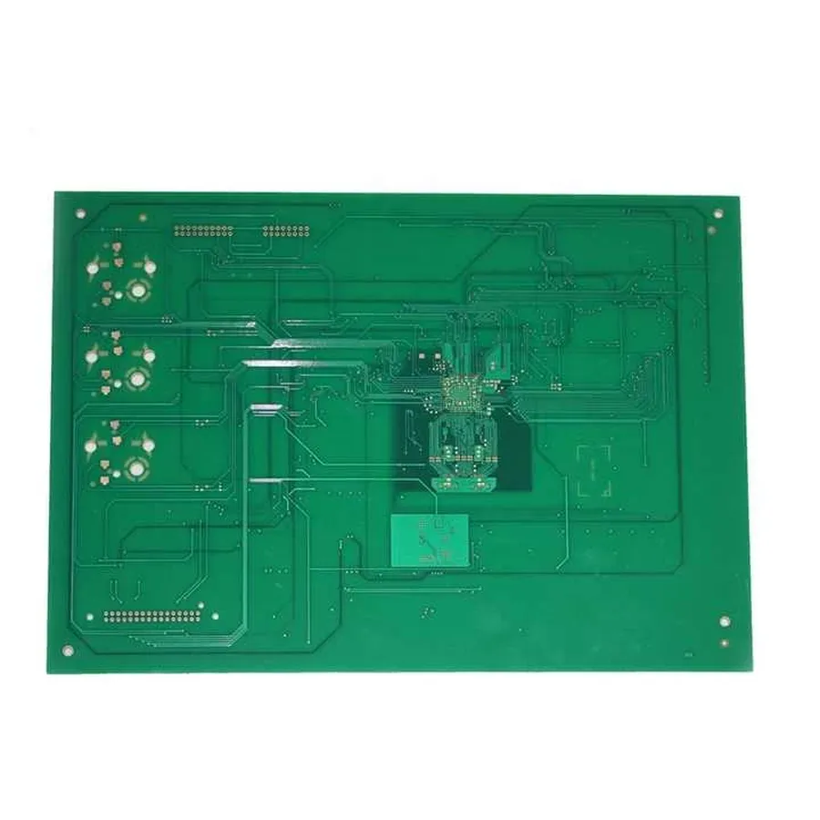
Accurately estimating your PCB design budget is crucial for project success, preventing unexpected costs and ensuring financial planning. This process involves understanding various cost drivers and applying a systematic approach to derive a realistic budget.
By carefully following these steps and considering the various factors, you can develop a realistic and detailed budget for your PCB design project, mitigating financial risks and enabling better project management.
| Checklist Item | Description |
|---|---|
| Project Requirements | Define clear specifications, functionality, and expected performance parameters of the PCB. |
| Complexity | Assess if the design involves a simple 2-layer board or a complex multi-layer board with high component density and specialized routing needs. |
| Component Count and Types | Determine the number and types of components used (basic, high-speed, BGA, etc.) |
| Board Size and Number of Layers | Specify dimensions of the board and the number of layers required for signal and power routing. |
| Routing Complexity | Analyze design parameters such as the need for high-speed routing, impedance control and differential pairs |
| Software and Licensing | Factor in expenses for PCB design software (Altium, KiCad, etc.) |
| Designer Expertise | Consider the experience and skills of the designer which affects design efficiency and costs. |
| Cost Model Options | Evaluate and compare hourly rate, project-based, or fixed-price contracts from designers or firms. |
| Contingency Funds | Include a 10-20% buffer to cover any unexpected changes or costs that may arise during the design. |
Understanding PCB design cost is crucial for effective project budgeting and successful product development. By examining the various factors influencing price, such as designer expertise, project complexity, software, and board layer counts, you can make informed decisions that balance quality and cost. Proper planning, effective communication with your designer, and exploring cost-effective design strategies are critical to ensuring a smooth development process while managing the overall 'pcb design cost'. Furthermore, the insights provided in this guide not only empower you to navigate the complexities of pcb design costs but also help you optimize your budget and achieve maximum value for your investment in electronics development.

