In today's rapidly evolving tech landscape, Printed Circuit Boards (PCBs) are the foundational building blocks of nearly every electronic device. Like the human nervous system, PCBs form the essential network that allows devices to function. Understanding the nuances of PCB prototype cost is crucial for inventors, engineers, and businesses. This article will illuminate the factors affecting PCB prototype cost, provide a comprehensive overview of available manufacturing options, and offer practical tips to effectively manage your project budgets. We'll also answer common questions about PCB prototype cost. Let's demystify this vital aspect of electronic product development together.
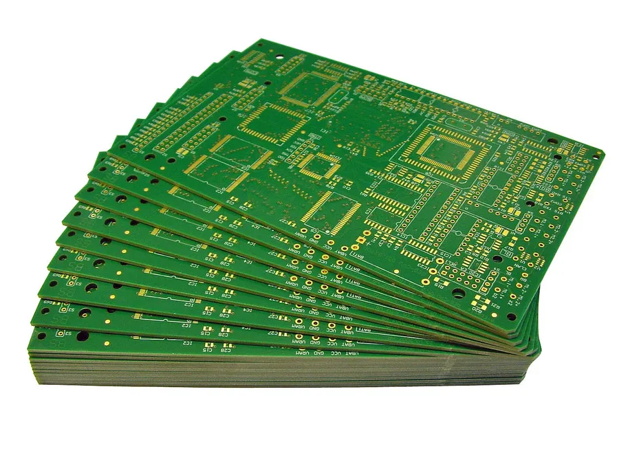
The cost of a PCB prototype is not a fixed value, it's a function of several interacting design and manufacturing parameters. Understanding these key factors is crucial for effectively managing your prototyping budget. These factors can be broadly categorized into design parameters, material selection, and fabrication processes.
| Factor | Description | Cost Impact |
|---|---|---|
| Board Dimensions | The physical size of the PCB. | Larger boards generally require more material and processing, increasing costs. |
| Layer Count | The number of conductive layers in the PCB. | More layers increase complexity and processing steps, resulting in higher costs. |
| Material Selection (e.g., FR-4, Rogers) | The base material of the PCB. | Standard FR-4 is cost-effective, while high-performance materials (e.g., Rogers) command a premium. |
| Surface Finish (e.g., HASL, ENIG) | The protective coating applied to copper pads. | HASL is a cost-effective finish, while ENIG (Electroless Nickel Immersion Gold) is more expensive but offers better performance. |
| Component Density | The quantity and proximity of electronic components on the board. | Higher component density can increase assembly complexity and cost. |
| Via Types (e.g., through-hole, blind, buried) | The type of connections between layers. | Blind and buried vias are more expensive to manufacture than through-hole vias. |
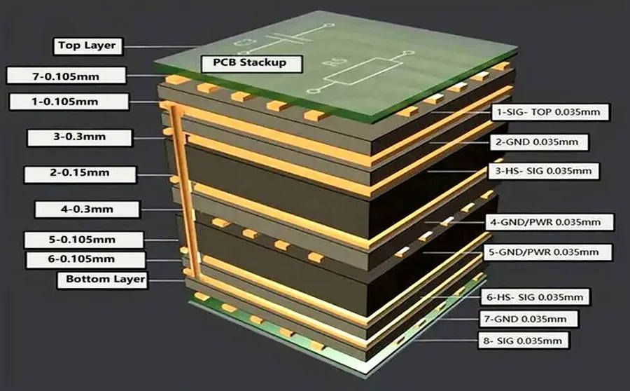
The complexity of a Printed Circuit Board (PCB) design is a significant determinant of its prototype cost. Intricate features such as high-density interconnects (HDI), blind and buried vias, and controlled impedance not only demand more sophisticated manufacturing processes but also necessitate tighter tolerances, leading to higher production expenses compared to simpler designs. These advanced requirements directly impact the cost of materials, fabrication, and testing.
| Complexity Feature | Impact on Cost | Reasoning |
|---|---|---|
| High-Density Interconnect (HDI) | High | Requires microvias, finer lines/spaces, more precise registration and specialized equipment. |
| Blind/Buried Vias | Medium to High | Increases manufacturing steps, adds complexity to drilling and plating processes. |
| Impedance Control | Medium | Demands precise trace width/spacing, requires specialized materials, controlled etching and additional testing. |
| Multiple Layers | Medium to High | Increases material cost, fabrication steps and complexity of alignment. |
| Complex Board Shape | Medium | Requires specialized routing tools and increases material wastage. |
| Fine Pitch Components | Medium to High | Demands high precision pick-and-place equipment, precise solder deposition and high accuracy inspection |
It's crucial to understand the trade-offs between design complexity and budgetary constraints. While advanced features can enhance performance and functionality, they also come at a premium. Designers must carefully evaluate the necessity of each complex feature against the overall project budget, and explore alternatives where possible.
The cost of a PCB prototype is significantly influenced by the manufacturing processes employed. Each fabrication method, from etching to drilling, carries its own cost profile and impacts the final price, with production scale playing a critical role in overall expenses.
| Process | Description | Cost Implications | Production Scale Impact |
|---|---|---|---|
| Etching | Removes copper from the board to create the desired circuitry. Typically uses chemical etchants. | Relatively low cost for simple designs, but costs can increase for very fine traces or complex patterns. | Economical at small scale, but becomes more cost-effective with larger batches due to efficiencies in process setup. |
| Photolithography | Uses light to transfer circuit patterns onto the PCB, enabling finer details and higher precision. | Higher initial setup costs compared to simple etching but allows for complex designs and tighter tolerances. | Benefits from scale as the tooling and setup costs are spread across more boards, reducing the per-unit cost. |
| Drilling | Creates holes for vias and component leads. Can be mechanical or laser drilling. | Mechanical drilling is cost-effective for larger holes and simpler designs, while laser drilling increases costs but allows for smaller and more precise holes. | Automated processes make larger drill volumes more cost effective. |
| Plating | Deposits a thin layer of metal (usually copper or tin) to enhance conductivity and solderability. | Chemical plating is a cost-effective option for less demanding applications, whereas electrolytic plating is more expensive, but allows more precise coating and better surface finishing. | Costs reduce per unit with larger batch sizes due to efficiency gains |
The choice of fabrication process is not solely determined by cost, it is also influenced by the technical requirements of the PCB. For instance, HDI boards necessitate photolithography and laser drilling, which inherently incur higher costs compared to simpler etching and mechanical drilling. Moreover, the selection of specific materials, such as those with higher glass transition temperatures, will also impact costs. For cost-effective prototyping, consider simplifying your design, opting for standard materials, and choosing cost effective surface finishes, whilst balancing functionality and manufacturability. For optimal pricing, it's critical to balance design complexity with cost considerations, understanding how different processes and scales can affect your project's budget.
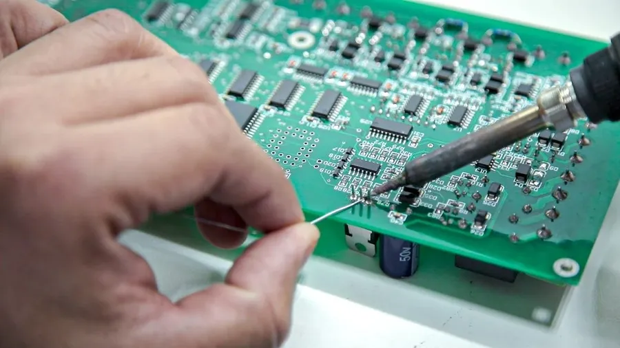
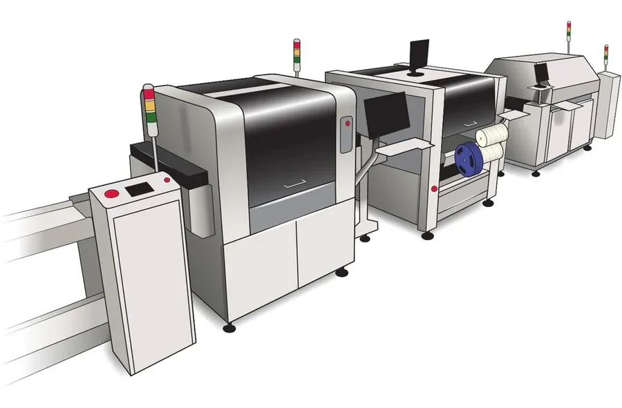
The cost of assembling a PCB prototype is significantly influenced by the price of electronic components and the labor involved in placing and soldering them onto the board. Understanding these cost drivers is crucial for effective budget management during PCB prototyping.
Component costs are highly variable and depend on factors including: * **Type of Component:** Resistors, capacitors, and basic logic chips are generally inexpensive, while complex integrated circuits (ICs), microcontrollers, and specialized sensors can be a significant portion of the cost. * **Quantity:** The number of each component used will directly affect the cost, with higher volumes leading to higher overall costs but potentially lower per-unit costs. * **Availability and Lead Time:** Components that are readily available in stock or have shorter lead times tend to be cheaper than components that are scarce or require a special order. * **Specific Characteristics:** Specific tolerance or precision requirements can drive up costs. Higher precision resistors, for example, will likely be more expensive. * **Supplier:** Prices can vary depending on where the components are purchased.
Labor costs are determined by the assembly method used. There are two main assembly methods: * **Surface Mount Technology (SMT):** Components are placed directly on the surface of the board. This method is typically faster and more efficient for higher volume runs and generally more cost-effective for smaller components. SMT assembly is often automated, which reduces labor costs. * **Through-Hole Technology (THT):** Components are inserted into holes on the board. This method is typically more labor-intensive and usually slower than SMT assembly. THT is often used for larger or mechanically stressed components where strong solder joints are necessary.
| Factor | Description | Cost Impact |
|---|---|---|
| Component Type | Basic components vs. Complex ICs | Highly variable, significant impact |
| Component Quantity | Number of parts on the board | Directly proportional to total component cost |
| Assembly Method | SMT vs. Through-hole | SMT typically less expensive, THT more labor intensive |
| Labor Rate | Hourly rate for assembly labor | Impacts the overall assembly cost |
Strategies to optimize assembly costs include: * **Standardization:** Using common, widely available components helps reduce material costs and lead times. Choosing components from the same manufacturer to reduce shipping costs. * **Design for Assembly (DFA):** Designing the board to simplify assembly reduces labor time. This includes using a consistent component size and orientation where possible and minimizing the number of through-hole components. * **Automated Assembly:** Where possible, use automated assembly methods for SMT to reduce labor time. * **Panelization:** Group multiple board designs together on one panel to reduce processing time. * **Order in Bulk:** Ordering larger quantities of components often reduces per-unit cost.
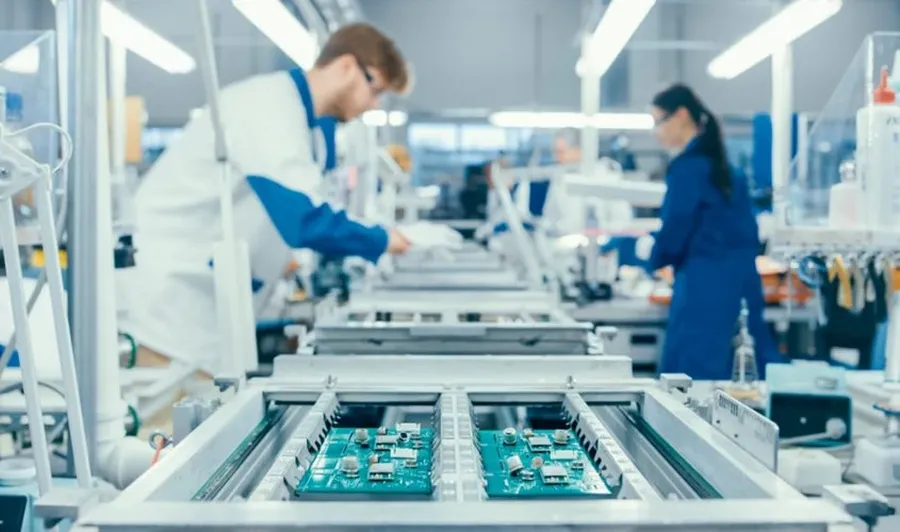
The geographic location of your PCB manufacturer significantly impacts prototype costs, quality, and turnaround time. Choosing between domestic (US), Chinese, or other international manufacturers requires careful evaluation of these key factors to balance budget with project requirements.
| Factor | USA | China | Other International |
|---|---|---|---|
| Cost | Higher, especially for small quantities | Significantly lower, especially for larger runs | Variable, often lower than US, may depend on labor and material costs |
| Quality | Generally high, often adheres to strict industry standards | Ranges from good to excellent; many manufacturers offer high-quality options | Variable; some may match US quality, while others may be lower |
| Turnaround Time | Relatively fast, usually within 1-2 weeks for prototypes | Can be very fast (days to 1 week) but also depends on shipping time | Variable, may be similar to or slower than China, depending on the country and manufacturer. |
| Communication | Generally easier due to language and time zone | May be challenging due to language barriers and time zone differences. | Varies significantly depending on language and time zone. |
| Intellectual Property (IP) Protection | Stronger IP protection laws and enforcement. | IP protection can be a concern; due diligence is critical. | Variable; depends on the country's legal framework. |
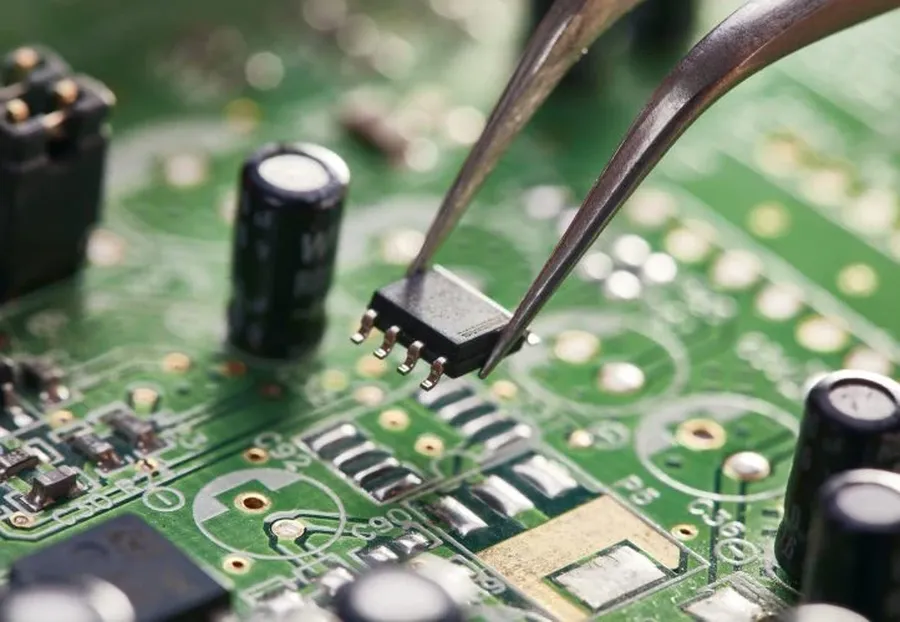
Reducing the cost of PCB prototypes is crucial for efficient product development. By strategically addressing design, component selection, and manufacturing processes, significant cost savings can be achieved without compromising quality or functionality. This section outlines actionable strategies for minimizing expenses associated with PCB prototyping.
The unit cost of PCB prototypes significantly decreases as the quantity of boards increases, a phenomenon driven by the economics of scale inherent in manufacturing processes. This principle holds true whether you're ordering a small batch of 5 boards or a larger production run; understanding these cost dynamics is crucial for effective budget management during the prototyping phase.
| Quantity | Unit Cost Trend | Setup Costs | Best Use Case |
|---|---|---|---|
| 1-5 Boards | Highest per unit | Distributed across few units | Initial design verification |
| 5-20 Boards | High to moderate per unit | Moderately distributed | Functional testing, small iterations |
| 20-100 Boards | Moderate per unit | Significantly distributed | Pilot runs, design refinement, early stage market testing |
| 100+ Boards | Lowest per unit | Insignificantly distributed | Small-scale production, pre-launch validation |
Ordering a small number of prototypes, such as 5 boards, incurs the highest per-unit cost because the initial setup costs (e.g., tooling, programming of machines) are spread across a small number of boards. Conversely, with a larger production run, these fixed costs are distributed across a greater number of units, driving down the cost per board. This does not mean that every project should strive for the highest number of boards, rather, projects need to strategically plan how many boards they need and how many boards they might need, to create the most cost efficient strategy.
Balancing prototyping needs with budget constraints involves carefully evaluating the purpose of your prototypes. For instance, if your primary goal is to validate the fundamental functionality of the design, a smaller quantity of boards might be sufficient. However, if you plan on running extensive tests or require multiple iterations of the design to fine tune performance, a larger quantity is more practical, even if it comes with a slightly higher initial investment. In addition, the cost of running multiple small runs vs a larger, single run needs to be taken into account; while a single large run could cost less, the risk is greatly increased if the design is not correct.
Understanding the costs associated with PCB prototyping is crucial for effective project planning and budget management. This section addresses frequently asked questions to provide clarity on various aspects influencing PCB prototype costs, offering practical insights for both novice and experienced users.
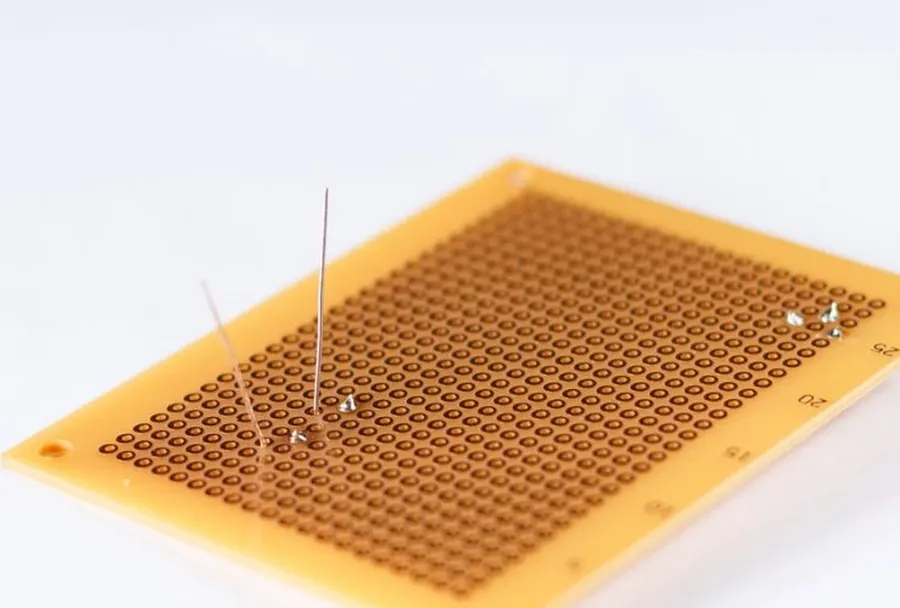
Analyzing real-world PCB prototype examples provides tangible insights into how various design and manufacturing choices affect cost. By examining specific cases, we can move beyond abstract principles and understand the practical implications of design decisions on the final price. These case studies will illustrate the cost differences between simple and complex designs, offering a benchmark for readers planning their own projects.
| Feature | Simple Prototype (Example 1) | Moderate Complexity Prototype (Example 2) | High Complexity Prototype (Example 3) |
|---|---|---|---|
| Board Dimensions | 50mm x 50mm | 100mm x 100mm | 150mm x 150mm |
| Layer Count | 2 Layers | 4 Layers | 8 Layers |
| Material | FR-4 Standard | FR-4 High Tg | FR-4 High Speed |
| Surface Finish | HASL | ENIG | ENIG |
| Vias | Through-Hole | Through-Hole and Blind Vias | Blind and Buried Vias |
| Component Density | Low (50 components) | Medium (200 components) | High (500+ components) |
| Special Features | None | Impedance Control | High-Density Interconnect (HDI) |
| Estimated Cost (5 units) | $50 | $300 | $1000 |
| Turnaround Time | 2 days | 5 days | 10 days |
| Typical Application | Basic LED circuit | Microcontroller board | High-speed communication module |
These examples illustrate the significant cost escalations that occur with increased design complexity. The 'Simple Prototype' represents a basic circuit and is the least expensive to produce. As complexity increases to 'Moderate' and then 'High,' the cost multiplies due to factors such as more complex manufacturing processes, specialized materials and a higher component count. The turnaround time also increases for complex PCBs due to the extra processing steps involved.
When planning a PCB prototype project, it's important to consider the trade-offs between design complexity and cost. Simple prototypes are a cost-effective way to test basic concepts and are ideal for projects without stringent requirements. For more advanced applications, the cost is often higher, reflecting the increased complexity and specialized manufacturing involved. These case studies offer a clear understanding of how the choices in design and manufacturing drive the price of PCB prototypes.
Navigating PCB prototype cost requires a thorough understanding of design complexities, manufacturing processes, and assembly options. Whether you're dealing with a simple circuit or a high-density design, every choice impacts the final cost. By understanding the factors mentioned and applying cost-reduction strategies, you can effectively manage your project budget and achieve your electronic innovation goals. Keep learning, stay updated on the latest pricing trends, and remember that the most cost-effective PCB prototype doesn't sacrifice quality. The knowledge to navigate [pcb prototype cost] will provide you a strong foundation for successful product development and future project planning.

