In today’s tech-driven world, printed circuit boards (PCBs) are the unsung heroes of almost every electronic device, from smartphones to sophisticated medical equipment. As the foundation of electronics, the cost of PCB fabrication is a crucial consideration for any project. A 'PCB fabrication quote' isn't just a number; it's a reflection of various design and manufacturing complexities. This article breaks down exactly what makes up a PCB fabrication quote, empowering you with knowledge to get the most cost-effective results for your printed circuit board project, ensuring the best path from blueprint to functional electronic reality.
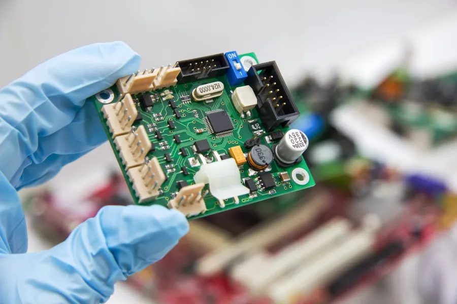
Understanding the primary drivers behind PCB fabrication costs is crucial for effective budget management and design optimization. The final price is a complex interplay of several factors, including material selection, the number of layers, board dimensions, quantity of boards ordered, and surface finishes. Each of these elements contributes uniquely to the overall expense, reflecting both the direct cost of materials and the complexity of the manufacturing processes involved.
| Factor | Impact on Cost | Description |
|---|---|---|
| Material Type | Significant | Different materials (e.g., FR-4, Aluminum, Polyimide) have varying costs due to material expenses and processing requirements. |
| Layer Count | Significant | Single-layer boards are the simplest and least costly, while multi-layer boards increase complexity and cost. |
| Board Dimensions | Moderate | Larger boards require more material and handling, leading to higher costs. |
| Quantity Ordered | Significant | Higher order quantities typically lower the per-unit cost due to economies of scale. |
| Surface Finish | Moderate | Finishes like ENIG are more expensive than HASL due to the materials and process complexity. |
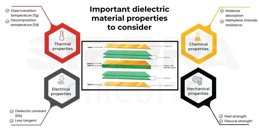
The choice of material for your printed circuit board (PCB) significantly influences both its performance and cost. Selecting the appropriate material requires a careful evaluation of the application requirements and budget constraints. This section will explore common PCB materials, highlighting their properties and how they factor into a PCB fabrication quote.
| Material | Description | Cost | Typical Applications | Advantages | Disadvantages |
|---|---|---|---|---|---|
| FR-4 | A composite material made of woven fiberglass cloth with an epoxy resin binder. It is the most common and versatile PCB material. | Low to Medium | General electronics, consumer devices, and most standard applications. | Cost-effective, widely available, good electrical insulation, and good mechanical strength. | Limited thermal performance, may not be suitable for high-frequency applications. |
| Aluminum | A metal core PCB with an aluminum base. It provides excellent thermal dissipation. | Medium to High | High-power LED lighting, automotive electronics, and power electronics. | Excellent thermal conductivity, good mechanical strength, and durable. | Higher cost, can be more complex to fabricate, and not suitable for high layer counts. |
| Polyimide | A high-performance polymer film material known for its heat resistance and flexibility. | High | Aerospace, medical, and high-temperature electronics. | Excellent temperature resistance, flexible, and good chemical resistance. | Higher cost, can be difficult to process, and sensitive to moisture. |
| Rogers Materials | A family of high-frequency laminates with low dielectric loss and stable electrical properties. | High | RF applications, high-speed digital circuits, and telecommunications. | Excellent electrical properties, low dielectric loss, and good for high frequencies. | High cost, requires specialized fabrication techniques, and more brittle. |
| CEM-1 | Composite epoxy material with a paper base, typically used as a cost-effective substitute for FR-4 for single layer boards. | Very Low | Low cost electronics, toys, and single layer boards. | Very cost-effective, easy to process. | Limited to single or double layer applications, not as strong as FR-4, and poor thermal and electrical properties. |
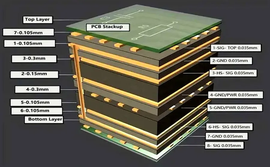
The number of layers in a PCB design is a primary cost driver, directly influencing both the material requirements and the manufacturing complexity, thereby significantly impacting the final PCB fabrication quote. Moving from a single-layer to a multi-layer board, the fabrication process becomes more intricate and requires specialized equipment and expertise, hence increasing costs. This section will delve into the complexities and cost implications associated with different layer counts.
| Layer Count | Complexity | Manufacturing Process | Cost Implications |
|---|---|---|---|
| Single-Layer | Simplest design | Basic fabrication with single-sided copper etching | Lowest cost option |
| Double-Layer | Moderate complexity | More involved than single-layer, requiring plating through holes and double-sided etching. | Moderate cost increase over single-layer PCBs |
| Multi-Layer (4+ Layers) | High complexity | Requires lamination, precise alignment, and specialized processes such as through-hole plating and via formation. | Higher cost due to increased material, equipment and processing requirements |
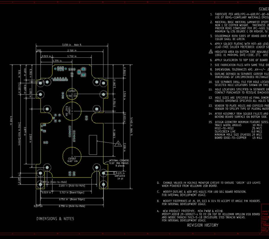
Printed circuit board (PCB) dimensions, thickness, and specified tolerances significantly influence both the final price and the manufacturing process. Optimizing these parameters is crucial for securing a cost-effective and producible PCB fabrication quote.
Understanding the interplay between these factors and their impact on cost enables you to engage in more effective negotiations with your PCB manufacturer.
| Parameter | Impact on Cost | Impact on Manufacturing | Optimization Strategies |
|---|---|---|---|
| Board Dimensions (Size and Shape) | Larger boards generally cost more due to increased material usage and processing time. Complex shapes can increase manufacturing complexity and cost. | Larger boards require more material handling and may have yield issues. Complex shapes require precision cutting and routing. | Minimize the board size to the required functionality. Simplify board shapes whenever possible. Panelize efficiently for production. |
| Board Thickness | Non-standard thicknesses may increase material cost and processing time. Thicker boards may incur higher material costs. | Thicker boards may present challenges in drilling and plating. Standard thicknesses streamline manufacturing processes. | Choose standard thicknesses when possible. Specify only the required thickness for application. Consult manufacturers for their standard available thicknesses |
| Specified Tolerances | Tighter tolerances increase manufacturing difficulty and require higher precision equipment which may increase cost. | Tighter tolerances demand more rigorous manufacturing processes and inspection. May increase production rejects and scrap. | Specify only necessary tolerances for functionality. Relaxing tolerances when appropriate reduces costs and improves yield. |
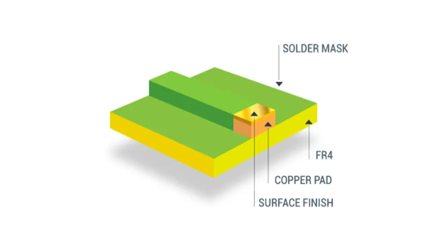
The selection of a surface finish for your printed circuit board (PCB) is a crucial step in the fabrication process, directly impacting cost, performance, and durability. This section explores common surface finish options, providing a comparative analysis to guide your decision-making when seeking a PCB fabrication quote. Choosing the right finish ensures optimal performance and reliability while aligning with your budget.
| Surface Finish | Description | Cost | Performance Characteristics | Typical Applications |
|---|---|---|---|---|
| HASL (Hot Air Solder Leveling) | A process where molten solder is applied to the exposed copper and leveled with hot air. | Low | Good solderability, cost-effective, but uneven surface can be an issue for fine pitch components. | General purpose PCBs, non-fine-pitch component applications. |
| ENIG (Electroless Nickel Immersion Gold) | Involves a layer of nickel followed by a thin layer of gold. Nickel provides a barrier and gold protects the nickel layer from oxidation. | High | Excellent solderability, flat surface, good for fine-pitch components, long shelf life. | High-reliability applications, fine-pitch and complex component assembly |
| OSP (Organic Solderability Preservative) | A thin, organic coating applied to the copper pads to protect them from oxidation prior to soldering. | Low | Good solderability, flat surface, cost-effective, but shorter shelf life and sensitive to handling and storage. | Mass production, consumer electronics, cost sensitive projects. |
| Immersion Tin | A thin layer of tin is deposited on the copper pads through a chemical process. | Medium | Good solderability, flat surface, suitable for fine-pitch components, but susceptible to tin whiskers. | Applications where environmental concerns restrict the use of lead |
| Immersion Silver | A thin layer of silver is deposited on the copper pads through a chemical process. | Medium | Excellent solderability, good conductivity, suitable for high-frequency applications but susceptible to tarnishing. | High-frequency applications and high-performance boards. |
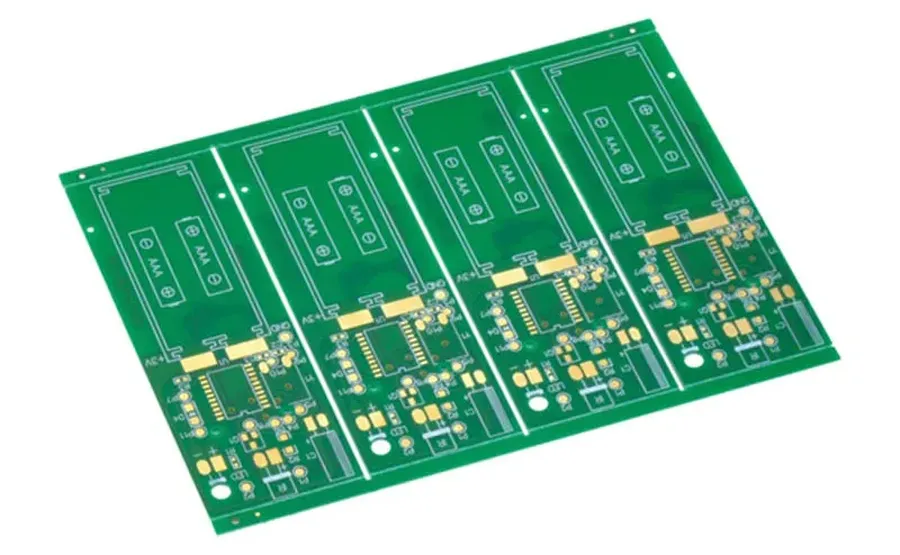
The quantity of printed circuit boards (PCBs) ordered is a primary factor influencing the per-unit cost. Larger production runs typically result in a lower price per board due to economies of scale, which is a fundamental principle in manufacturing.
The reduction in per-unit cost with increased quantity stems from several aspects of the PCB manufacturing process. These include: reduced setup costs amortized over a larger number of boards, more efficient use of materials, and optimized machine operation. This effect is particularly noticeable when comparing small prototype runs to large production orders.
| Order Quantity | Per-Unit Cost | Setup Cost Amortization | Material Usage Efficiency |
|---|---|---|---|
| 1-10 boards | High | High per unit | Lower efficiency, more waste |
| 100-500 boards | Medium | Moderate per unit | Medium efficiency, some waste reduction |
| 1000+ boards | Low | Very low per unit | High efficiency, minimal waste |
The relationship between order quantity and unit price is not always linear. There are often tiered pricing structures where significant price breaks occur at specific quantity thresholds. Understanding these thresholds is key to optimizing your order and reducing your overall PCB fabrication quote. For example, going from 900 to 1000 pieces might dramatically reduce the unit price, while the unit price reduction might be minimal when going from 1000 to 1100 pieces.
Lead time, the duration from placing an order to receiving the finished PCBs, significantly impacts fabrication costs. Expedited manufacturing, which shortens lead times, typically incurs additional charges. Balancing the need for speed with budgetary constraints is critical when obtaining a PCB fabrication quote. This section will explain the nuances of lead times, their effects on pricing, and provide guidance on making informed decisions to get the best quote for your printed circuit board needs.
The relationship between lead time and cost is generally inversely proportional. Standard lead times allow manufacturers to schedule production more efficiently, reducing costs. However, shorter lead times require expedited handling and processing, leading to increased expenses. Therefore, it is essential to understand the different lead times and their price points when planning your project.
| Lead Time Option | Typical Lead Time | Cost Implication | Suitability |
|---|---|---|---|
| Standard | 1-2 weeks | Lowest | Projects with flexible deadlines |
| Express | 3-7 business days | Moderate increase | Projects with moderately tight deadlines |
| Expedited | 24-72 hours | Highest | Projects with critical deadlines or prototypes |
Several factors may influence the quoted lead time. These may include the complexity of the PCB, the required materials, the manufacturer's current workload and capacity, and any special manufacturing requirements such as surface finish or testing. Be prepared for these factors to be reflected in lead times as well as prices.
When negotiating your PCB fabrication quote, prioritize an appropriate lead time that aligns with your project needs. If a delay in project completion is acceptable, opting for standard lead times offers significant cost savings. On the other hand, if the project demands urgent delivery, carefully evaluate expedited options while keeping your budget in mind. Planning ahead and accounting for lead time requirements will help you receive a better quote.
Beyond the base cost of PCB fabrication, several surcharges and additional costs can significantly impact the final price. These often arise from specific design needs, quality requirements, or material choices, and understanding them is crucial for accurate budgeting and avoiding unexpected expenses when evaluating a PCB fabrication quote. These costs are a function of the complexity of your board's specifications and the manufacturing process it requires.
Navigating the world of PCB fabrication quotes can be complex. This section addresses common questions to help you understand the factors influencing cost and how to secure the best possible quote.
Understanding the intricacies of a 'PCB fabrication quote' is crucial for effectively managing project costs and timelines. By considering all aspects, from material selection to lead times, you can secure the best possible pricing for your project while upholding the quality of your printed circuit boards. Remember, the most cost-effective quote balances price with performance, ensuring a smooth transition from design to reality, with reliable and efficient PCB fabrication.

