
Electronic Power Steering (EPS) systems are the backbone of modern vehicle maneuverability, demanding flawless performance under extreme thermal and vibration stress. As automotive architectures evolve toward autonomy, the margin for error in PCB design has vanished. This guide provides an authoritative roadmap to mastering the technical intricacies of EPS circuit design, ensuring your boards not only pass rigorous validation but excel in the field.
The Anatomy of High-Reliability EPS Systems
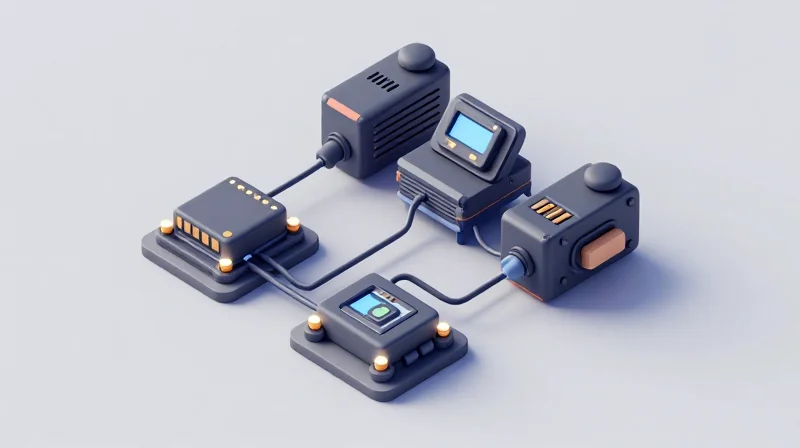
The Operational Demands of EPS Control Units
Electronic Power Steering systems operate at the critical intersection of vehicle dynamics and safety. Unlike infotainment or comfort electronics, EPS PCB assemblies must maintain continuous functionality during transient voltage spikes, high thermal stress, and intense electromagnetic interference. The architecture of these modules is predicated on the necessity of high current handling for motor phase control alongside precision sensor signal conditioning for steering torque inputs.
Key Environmental Stress Factors
| Stress Factor | Impact on PCB Design | Mitigation Strategy |
|---|---|---|
| Thermal Cycling | Solder joint fatigue and delamination | CTE-matched substrates and enhanced underfill |
| Transient Voltages | Dielectric breakdown and logic failure | Multistage TVS diode suppression |
| Vibration/Shock | Interconnect failure and component fatigue | Rigid-flex construction and optimized anchoring |
Safety Integrity and ASIL Compliance
Achieving Automotive Safety Integrity Level (ASIL) D requires a hardware architecture that inherently supports fault detection and isolation. This involves redundant power supply rails, cross-checked microcontroller pathways, and the implementation of sophisticated diagnostic coverage (DC) through hardware-based monitors. The PCB design must ensure that no single point of failure can lead to an uncontrolled steering state.
- How does ASIL D influence PCB layout?
Layout must enforce strict physical and electrical isolation between redundant safety channels to prevent common-cause failures induced by localized shorts or heat zones. - What is the primary concern for power stage design?
Thermal management and low-impedance current paths are vital to minimize switching losses and prevent thermal runaway during peak steering assist demand. - Why is electromagnetic compatibility (EMC) so critical here?
EPS units are often located in high-noise environments; insufficient filtering can corrupt sensitive low-voltage torque sensor data, leading to erroneous steering interventions.
Advanced Thermal Management Strategies
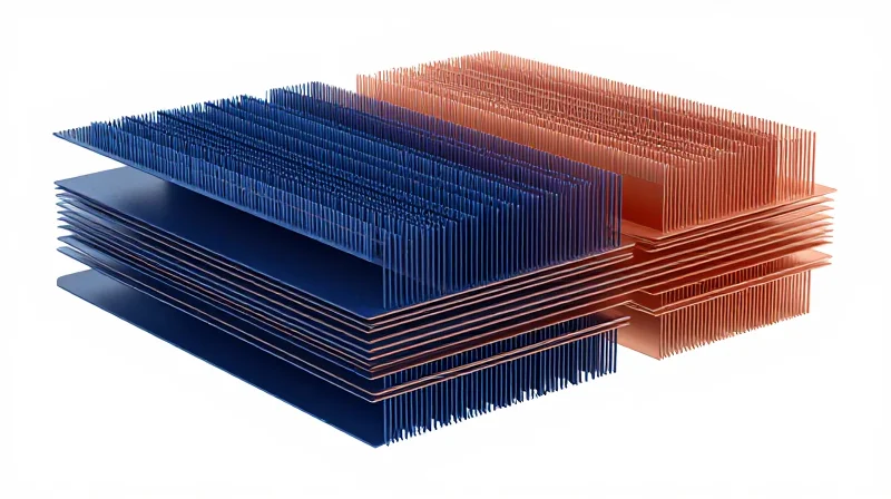
Thermal Dissipation Strategies for EPS Assemblies
Efficient thermal management in EPS units requires a multi-layered approach that bridges the gap between high-current electrical demands and the physical constraints of an automotive engine-room housing. Given the high ASIL requirements, reducing junction temperatures is not merely a design preference but a prerequisite for component longevity and system stability under peak load.
Material and Layout Optimization
| Strategy | Primary Benefit | Technical Consideration |
|---|---|---|
| Heavy Copper (3oz+) | Lowers trace resistance and I2R losses. | Requires adjusted etching parameters for impedance. |
| Thermal Vias | Conducts heat to internal ground planes. | Must be capped/filled to prevent solder wicking. |
| Strategic Component Placement | Prevents thermal hot-spot coupling. | Requires CFD analysis for airflow paths. |
Thermal Engineering Best Practices
- How do copper weights influence thermal reliability?
Increasing copper weight from standard 1oz to 3oz or 4oz significantly lowers the thermal impedance of the substrate, allowing for better heat spreading across the entire PCB surface and preventing localized thermal runaway near MOSFET stages. - What role do thermal vias play in dense EPS housings?
Thermal vias act as heat pipes, moving energy from the component pads directly into the internal ground plane layers. For high-reliability designs, these should be arranged in a tightly packed array directly underneath power-dissipating elements. - How should components be grouped for optimal thermal management?
High-heat generating components like MOSFETs and shunt resistors should be physically decoupled from sensitive microcontroller and logic signal lines to prevent heat soak from impacting clock stability and signal integrity.
Mastering Signal Integrity in High-Current Environments

Mitigating Electromagnetic Interference in EPS Assemblies
High-current switching within an Electronic Power Steering (EPS) system generates significant electromagnetic interference (EMI) that can compromise sensitive logic circuitry. To maintain system reliability under ASIL-D safety requirements, engineers must employ a low-inductance loop design that physically isolates high-power motor phases from low-voltage signal traces. By minimizing current loop areas, designers inherently reduce radiated emissions and susceptibility to coupling, which is critical when the PCB resides in a compact automotive housing.
Strategic PCB Stack-up and Routing Protocols
Optimal signal integrity is achieved by implementing a multi-layer stack-up where signal layers are tightly coupled to solid ground planes. Utilizing differential pair routing for critical sensor feedback, such as torque or motor position signals, provides immunity to common-mode noise. Designers should adhere to the following routing standards to ensure stable performance:
- Trace Separation
Maintain a minimum distance of three times the dielectric height (3H) between high-speed signal traces to significantly reduce crosstalk. - Ground Plane Integrity
Ensure ground planes remain continuous beneath high-frequency signal paths to provide a low-impedance return current path, preventing loop-induced EMI. - Vias and Stubs
Minimize the use of vias in high-speed paths and eliminate long trace stubs to prevent signal reflections and resonance issues.
Comparative Analysis: EMI Mitigation Techniques
| Methodology | Effectiveness | Implementation Complexity |
|---|---|---|
| Differential Pair Routing | High (Common-mode rejection) | Moderate |
| Stitched Shielding Vias | High (Radiated emissions) | Low |
| Buried Capacitance | Moderate (Noise suppression) | High |
FAQ: Signal Integrity in High-Current EPS
- How do you prevent motor phase noise from coupling into the logic gates?
Physical isolation combined with guarded signal traces and the implementation of RC filters near the microcontroller inputs are essential to suppress noise before it enters the digital domain. - Why is layer stack-up critical for high-current EPS boards?
A well-designed stack-up dictates the impedance control and return current paths; improper layer ordering can lead to increased parasitic inductance, causing voltage spikes that could damage sensitive EPS components.
Essential DFM Rules for Automotive Yields
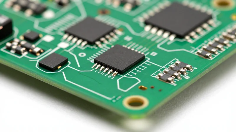
Optimizing Pad Geometry and Solder Mask Dams
For automotive-grade EPS controllers, pad design must balance mechanical strength with solder joint reliability. Standard practice involves implementing non-solder mask defined (NSMD) pads for small-pitch ICs to ensure superior solder adhesion, while solder mask dams must be strictly maintained at a minimum of 0.075mm to prevent bridging during high-volume reflow processes.
| Feature | Recommended Constraint | EPS Reliability Impact |
|---|---|---|
| Solder Mask Dam | ≥ 0.075 mm | Prevents electrical shorts during reflow |
| Pad-to-Pad Clearance | ≥ 0.150 mm | Minimizes parasitic effects and bridging risk |
| Trace Width (Power) | ≥ 0.300 mm | Ensures current carrying capacity |
DFM Best Practices for EPS Assembly Reliability
- How does component orientation affect yield?
Components should be oriented parallel to the direction of wave soldering to minimize shadow effects and prevent uneven solder distribution. - What is the critical rule for via-in-pad usage?
Via-in-pad must be plugged and capped with conductive or non-conductive epoxy to avoid solder wicking, which creates voids and brittle joints under automotive vibration stress. - Why is copper balancing essential?
Asymmetric copper distribution leads to board warpage during the thermal cycling of reflow, compromising the integrity of BGA connections.
Automated Design Verification
To enforce these standards, integrate the following design rules into your automated DFM check suite to ensure every EPS assembly meets automotive IPC-Class 3 requirements.
DRC_RULE_MIN_MASK_DAM = 0.075mm
DRC_RULE_MIN_GAP = 0.150mm
DRC_RULE_VIA_IN_PAD = CAPPED_AND_PLUGGED
ENFORCE_COPPER_BALANCE = TRUE
Materials and Laminates for Harsh Environments
High-Tg Substrates for Thermal Resilience
Under-the-hood EPS applications subject PCBs to extreme temperature fluctuations, often ranging from -40°C to +150°C. Standard FR-4 laminates fail due to the mismatch between the Coefficient of Thermal Expansion (CTE) of the dielectric and the copper interconnects, leading to barrel cracking in vias and delamination. Engineers must specify high-Tg (glass transition temperature) materials, typically exceeding 170°C, to maintain structural integrity and electrical stability under continuous thermal stress.
| Parameter | Standard FR-4 | High-Tg Automotive Grade |
|---|---|---|
| Tg (°C) | 130-140 | >170 |
| Td (°C) | 300 | >340 |
| CTE Z-Axis (ppm/°C) | 4.0 - 5.0 | <3.0 |
| Thermal Shock Resistance | Low | Very High |
Material Selection Considerations
- Why is the Z-axis CTE critical for EPS boards?
A low Z-axis CTE prevents the vertical expansion of the laminate from fracturing plated through-holes (PTH) during the rapid heating and cooling cycles inherent in automotive power steering operation. - How do CAF (Conductive Anodic Filament) resistant materials impact reliability?
CAF-resistant resins inhibit the growth of conductive filaments between closely spaced copper features, which is essential for high-density EPS boards where high voltage/current leads to potential electrochemical migration. - What role does Td (Decomposition Temperature) play?
A high Td ensures the laminate can withstand the high-temperature profiles required for modern lead-free solder reflow processes without chemical degradation.
Manufacturing Best Practices
Beyond material selection, DFM success depends on surface finish and solder mask compatibility. For EPS assemblies, Electroless Nickel Immersion Gold (ENIG) or Immersion Silver (ImAg) provides superior planarity for high-power components. Furthermore, implementing a 'Solder Mask Dam' of at least 75-100μm is mandatory to prevent solder bridging between fine-pitch motor drive ICs, ensuring that the laminate's thermal performance is not compromised by latent short-circuit risks.
Ensuring Robustness Against Vibration and Mechanical Stress
Mitigating Mechanical Fatigue in High-Vibration Environments
Automotive power steering systems are subject to continuous harmonic oscillations and shock loads that can induce premature solder joint fatigue. Achieving mechanical robustness requires a holistic design strategy that combines optimized board layout, strategic component placement, and advanced solder joint reinforcement. By minimizing board deflection and stress concentrations, engineers can ensure long-term reliability in the harshest under-the-hood environments.
Strategic SMT Securement Techniques
For heavy or high-mass surface-mount devices (SMDs), standard solder fillets are often insufficient to prevent failure under G-force stress. Implementation of secondary mechanical stabilization is mandatory for components such as inductors and large electrolytic capacitors.
- Underfill Application
Utilize capillary underfill for BGA and CSP components to distribute thermal expansion stress and mechanical shock loads evenly across the package, significantly reducing strain on solder balls. - Corner Staking
Apply high-modulus, thermally stable structural adhesives at the corners of high-mass SMDs to decouple mechanical stress from the solder interconnects. - Through-Hole Retention
Where possible, leverage through-hole pins for high-mass components to provide primary mechanical anchoring, leaving the solder joints as secondary electrical connections.
PCB Board Edge and Support Design
| Feature | Design Specification | Reliability Impact |
|---|---|---|
| Board Edge Clearance | Minimum 2.5mm from trace | Prevents copper tearing during depaneling |
| Mounting Hole Proximity | Pad offset > 3mm | Reduces local PCB flexure stress near screws |
| PCB Support Standoffs | Grid spacing < 50mm | Increases resonant frequency, avoiding mechanical flutter |
The board edge should be treated as a high-stress zone. Routing traces parallel to the edge of the board, especially near mounting points, increases susceptibility to delamination under vibration. Ensure a keep-out zone for signals and vias to protect the integrity of the substrate.
Testing, Validation, and Quality Compliance
Advanced Validation Strategies for EPS Assemblies
For Electronic Power Steering (EPS) systems, validation is not merely a final stage but an iterative process integrated into every phase of the PCB lifecycle. Compliance with IPC-6012 Class 3 performance requirements is mandatory, necessitating robust inspection protocols that surpass standard consumer-grade electronics.
| Test Methodology | Primary Objective | Frequency/Standard |
|---|---|---|
| Automated Optical Inspection (AOI) | Detect surface defects and alignment | 100% In-Line |
| In-Circuit Testing (ICT) | Verify electrical connectivity and values | 100% Production |
| Thermal Cycling (-40°C to +125°C) | Identify fatigue and CTE mismatch | AEC-Q100/AEC-Q200 |
| X-Ray Inspection | Assess BGA/QFN solder joint integrity | Sampling/Critical SMT |
Compliance and Quality Assurance
Adherence to IPC standards ensures that the PCB can withstand the high-current demands and vibration environments inherent in steering systems. Validation protocols focus on internal layer registration, plating thickness, and dielectric strength to prevent latent failures in the field.
- How does IPC-6012 Class 3 improve EPS reliability?
Class 3 provides stricter acceptance criteria for hole fill, annular ring requirements, and conductor width tolerances, ensuring consistent performance in mission-critical applications. - Why is 100% X-ray inspection critical for EPS?
BGA and QFN components used in power modules can harbor hidden solder voids; X-ray is the only non-destructive method to ensure adequate solder volume and electrical contact. - What role does thermal shock testing play in DFM?
It validates that the laminate materials and copper plating can survive repeated expansion and contraction cycles without developing micro-cracks or barrel cracking.
Designing for EPS is a balancing act between power density and long-term durability. By strictly adhering to these DFM principles, engineering teams can minimize field failures and optimize production costs. Ready to elevate your next automotive project? Contact our engineering team today to review your board specifications and ensure your EPS design meets the highest industry standards.
