
Designing electronics for the rugged, high-voltage environment of welding machinery presents unique challenges. When a control board fails, the cost of downtime is catastrophic. This guide explores the critical DFM (Design for Manufacturing) strategies required to build robust, high-current PCBs that withstand severe electrical surges and thermal stress.
The Physics of High-Current PCB Reliability
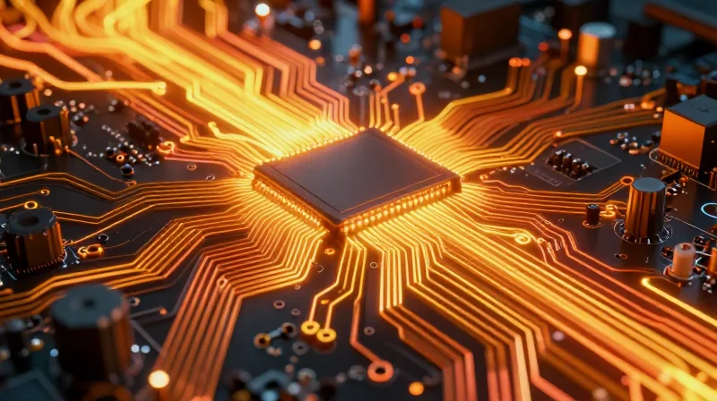
The Thermal-Electrical Interplay
In high-current environments such as welding power supplies, PCBs must act as robust power conductors rather than mere signal carriers. The fundamental physics governing these designs is Joule heating, where power dissipation is defined by the formula $P = I^2R$. When current flows through a copper conductor, any resistance—however minute—is amplified quadratically by the current load. This heat accumulation triggers a degradation cycle: increased temperature elevates the copper's resistivity, further increasing heat output and potentially leading to delamination, solder joint fatigue, or track fusion.
Material Impact on Current Capacity
| Parameter | Effect on Reliability | Design Strategy |
|---|---|---|
| Copper Thickness | Higher cross-sectional area reduces resistance | Use 2oz to 4oz copper for primary power paths |
| Trace Width | Directly determines current carrying capacity | Follow IPC-2221/IPC-2152 standards for sizing |
| Thermal Vias | Conducts heat away from copper planes | Use dense arrays under power MOSFETs |
Technical Considerations for High-Current Layout
- How does surface finish affect power reliability?
While ENIG is common for fine-pitch components, high-current areas should prioritize thick OSP or HASL/Immersion Silver to ensure a robust mechanical bond between the copper trace and the high-amperage terminal or connector. - What role does substrate choice play?
Standard FR-4 may become unstable at the operating temperatures of high-load welding circuits; high-Tg (glass transition temperature) materials are essential to maintain mechanical integrity under persistent thermal stress. - Is internal layer current density safe?
Internal layers have significantly lower heat dissipation compared to outer layers. It is best practice to move high-current paths to the outer layers where convective cooling is most effective.
Best Practices for Trace Geometry
To minimize inductance and resistive losses, paths must be as short and wide as possible. Avoid 90-degree bends in power paths, as they create current density hotspots and electromagnetic radiation. Instead, use 45-degree angles or curved traces to ensure uniform current distribution across the copper cross-section.
Mastering Thick Copper Plating and Weight Requirements
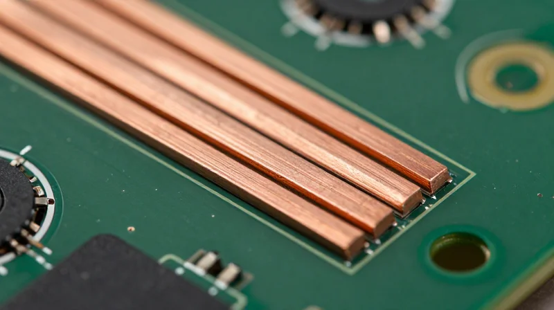
Optimizing Trace Geometry for High-Current Capacity
In welding equipment, where currents often exceed 50A, standard 1oz copper is insufficient. Utilizing 3oz to 6oz copper weight significantly increases the cross-sectional area of the conductors, directly lowering ohmic resistance and reducing energy loss as heat. When designing for high current, the PCB layout must account for both the copper thickness and the trace width to ensure the current density stays within the thermal limit of the laminate material.
| Copper Weight | Relative Resistance | Typical Application in Welders | Thermal Management |
|---|---|---|---|
| 1 oz | 1.0x (Baseline) | Control/Signal paths | Poor for high current |
| 3 oz | 0.33x | Secondary power stages | Moderate heat dissipation |
| 6 oz | 0.16x | Main welding output bus | Excellent heat dissipation |
Key Considerations for 3oz+ Copper Designs
- How does copper weight affect trace spacing?
As copper thickness increases, the etching process requires wider spacing between traces to maintain integrity and prevent undercut issues, impacting routing density. - Can I use standard via structures for 6oz copper?
No, high-current paths require stitched via arrays or press-fit pins to handle the massive current density that a single standard via would fail to conduct. - What is the impact on solder mask?
Thick copper creates significant topographical height differences; applying a high-build solder mask or using specialized thermal interface materials is critical to ensure proper insulation and coverage.
Designers must balance the PCB board real estate with thermal requirements. For heavy-duty welding machines, prioritize 6oz copper for the primary power bus, while transitioning to 3oz for auxiliary power paths to optimize both cost and performance.
Precise Trace Width Calculations: Beyond IPC-2221
Limitations of Standard IPC-2221 Estimations
While IPC-2221 provides a fundamental baseline for trace sizing, it often fails to account for the aggressive thermal profiles found in welding equipment. Standard calculators assume steady-state operation at ambient temperatures, ignoring localized heating effects from power semiconductors and the poor heat-sinking properties of thick, plastic-encased chassis. Relying strictly on these formulas can lead to under-dimensioning, resulting in catastrophic insulation breakdown or solder joint fatigue.
Real-World Correction Factors
| Variable | Influence on Trace Size | Adjustment Strategy |
|---|---|---|
| Ambient Temp (>50°C) | High | Derate current capacity by 15-20% |
| Copper Purity | Moderate | Use 95% conductivity factor for standard ETP copper |
| Pulse Loadings | Critical | Base width on RMS current, verify with peak current spikes |
| Conformal Coating | Low to Moderate | Account for 5°C thermal impedance rise |
Advanced Calculation Considerations
To achieve high reliability, designers must integrate finite element analysis (FEA) or secondary empirical data alongside IPC standards. Key design adjustments include:
- Thermal Coupling
Traces should be spaced to prevent cumulative thermal 'hot zones' where adjacent high-current paths raise the effective board temperature beyond the base ambient calculation. - Copper Weight Variance
Manufacturing tolerances for thick copper (e.g., 3oz+) can result in 10-15% thickness reduction at the trace edges; always use a 90% effective thickness value for calculations. - Duty Cycle Integration
Welding machines operate on varying duty cycles; use the RMS equivalent of the weld current curve rather than peak current for steady-state trace sizing.
FAQ: Trace Width and Current Management
- Should I use IPC-2221 or IPC-2152?
IPC-2152 is scientifically superior as it relies on empirically derived data and accounts for a wider variety of board geometries and thermal environments than the older IPC-2221. - How does PCB thickness affect my calculation?
Thicker boards (e.g., 2.4mm vs 1.6mm) have different thermal mass properties and heat dissipation paths; always simulate the total stack-up to verify thermal equilibrium.
Thermal Dissipation Strategies for High-Power Boards
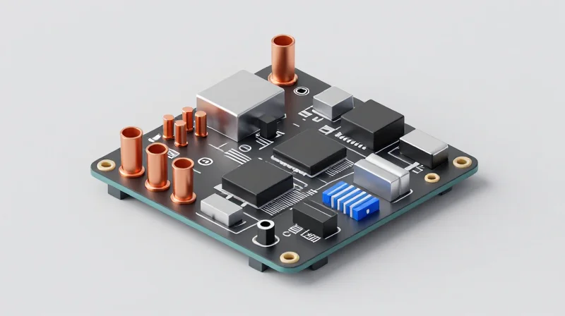
Managing Heat Dissipation in Industrial Welding PCBs
Thermal management in high-current welding environments is not merely about adding a heat sink; it involves designing the board itself as a heat conduction path. By optimizing the PCB's thermal resistance, designers can prevent localized hotspots that accelerate substrate aging and solder joint fatigue.
Thermal Via Arrays and Ground Planes
Thermal vias act as vertical heat pipes, moving energy from surface-mount power devices into internal copper planes. For maximum efficiency, these vias should be plated with high-conductivity copper and localized directly beneath the component's thermal pad. Using a dense grid of stitching vias can effectively turn a standard ground plane into a robust heatsink.
| Strategy | Primary Benefit | Implementation Tip |
|---|---|---|
| Thermal Vias | Vertical heat conduction | Fill with conductive epoxy |
| Large Copper Pours | Lateral heat spreading | Maintain clearance for creepage |
| Component Staggering | Reduced localized heating | Avoid grouping high-wattage components |
Frequently Asked Questions
- Does PCB thickness affect thermal dissipation?
While thicker substrates (e.g., 2.4mm or 3.2mm) provide better mechanical rigidity for heavy welding transformers, they can sometimes act as insulators, making copper-to-copper thermal pathing more critical. - Are filled and capped thermal vias necessary?
Yes, for high-power applications, filling vias with thermally conductive material prevents solder wicking into the barrels during assembly, ensuring a solid thermal contact. - How does PCB finish impact heat transfer?
ENIG is preferred for its flatness, but OSP or HASL are often used on power boards to allow for higher solder volume, which assists in thermal conductivity through increased contact area.
Preventing Catastrophic Failure During Voltage Surges
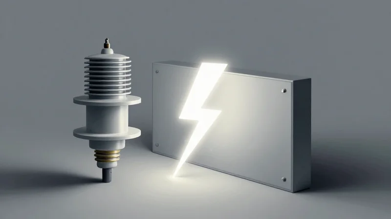
In welding environments, transient voltage surges are not merely theoretical risks but operational certainties. When designing high-current PCBs for these applications, failure to implement proper protection leads to immediate dielectric breakdown, carbon tracking, and explosive failure of copper traces. Effective design must prioritize the integrity of the insulation material and the implementation of fast-acting surge diversion paths.
Mitigating Dielectric Breakdown and Arcing
Arcing occurs when the voltage potential exceeds the dielectric strength of the PCB substrate or the surrounding air gap. To prevent this, designers must move beyond standard low-voltage spacing rules. Incorporating physical slots (milling) between high-potential regions and ground planes effectively increases the creepage path distance, which is far superior to relying solely on surface distance across a laminate.
| Requirement Type | Strategy for Welding PCBs | Benefit |
|---|---|---|
| Creepage Distance | Increase beyond IPC-2221 | Prevents surface arcing due to dust/moisture |
| Slot Milling | Remove material between nodes | Maximizes dielectric strength in limited space |
| Conformal Coating | Use high-dielectric acrylic/silicone | Protects against conductive welding debris |
Surge Protection Component Integration
The primary defense against transient surges in welding power stages is the strategic placement of Metal Oxide Varistors (MOVs) and Transient Voltage Suppressors (TVS). These components must be placed as close to the board entry point as possible to clamp voltage spikes before they propagate through sensitive logic or control circuitry.
- Why is trace geometry critical near surge arrestors?
Traces connecting MOVs must be kept extremely short and wide to minimize parasitic inductance, which otherwise negates the clamping speed of the protection device. - How does delamination occur during surges?
Rapid heat generation from an arc causes localized expansion of the FR-4 resin. If the copper-to-substrate bond is weak or the thermal stress is too high, the layers will separate, leading to permanent board failure. - Is internal layer clearance different from outer layers?
Yes. Internal layers have higher dielectric stability, but they remain susceptible to 'tracking' if carbonization occurs during a surface fault; always maintain wider margins on external layers.
/* Recommended Clearance Rule for High Voltage Nodes */
// For peak voltages > 500V in welding environments
// Clearance = (Voltage / 100) * 1.5mm
// Ensure a minimum 5mm air gap for bare HV pads
Strategic Stack-up Planning for Power Planes
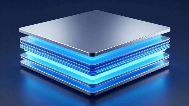
Optimizing Layer Assignments for High-Current Density
In welding machine controllers, the stack-up must prioritize low-impedance current paths while isolating sensitive analog feedback circuits. By placing high-current power planes in the internal layers—surrounded by ground planes—you minimize radiated emissions and stabilize the voltage rail against the inductive kickback common in welding operations.
| Layer Function | Recommended Placement | Design Priority |
|---|---|---|
| High-Current Power | Internal Mid-Layers | Thermal distribution and EMI shielding |
| Signal / Feedback | Inner Signal Layers | Proximity to ground plane for return paths |
| High-Voltage Planes | Top/Bottom with isolation | Creepage and clearance maintenance |
Critical Considerations for Power Plane Balancing
Asymmetric stack-ups are a frequent cause of PCB warping during the reflow process, which can lead to mechanical stress on large high-current connectors. To maintain mechanical stability, ensure that copper distribution is balanced across the vertical axis of the board.
- Why should I use heavy copper on internal layers?
Internal layers provide better heat dissipation across the entire board surface, whereas external traces rely heavily on convection and solder mask emissivity. - How does stack-up affect signal noise?
Placing a solid ground plane directly adjacent to high-speed signal layers creates a low-impedance return path, significantly reducing loop area and electromagnetic interference. - Can I mix low-power and high-power planes?
It is generally discouraged. If unavoidable, maintain strict horizontal separation (split planes) and ensure return paths do not cross the gap between different power domains.
Best Practices for Stack-up Documentation
When communicating with your PCB fabricator, always specify the required dielectric constant (Dk) and copper weight per layer. For welding applications, requesting controlled impedance and thermal via stitching guidelines in the fabrication notes prevents costly misinterpretations and ensures long-term operational reliability.
DFM Checklist for PCB Fabrication Success
Critical DFM Fabrication Checklist
Fabrication success for high-current welding PCBs depends on tight tolerance control and material selection. Ensure your design files reflect these manufacturing-ready specifications to avoid production stalls or field failures.
- Mask Clearance and Registration
Ensure a minimum solder mask dam of 0.1mm between high-voltage pads. Excessively small clearances increase the risk of bridging and arcing during operational voltage surges. - Copper Weight Consistency
Specify heavy copper (2oz to 4oz+) clearly in the fabrication drawing. Verify that the fabricator can support the required plating thickness in internal layers without compromising hole wall integrity. - Edge Plating and De-burring
For high-current designs where board edges are used as mounting or thermal contact points, ensure edge plating is specified to enhance thermal conductivity and edge robustness. - Surface Finish Selection
Avoid OSP for high-current applications. Electroless Nickel Immersion Gold (ENIG) or Immersion Silver are preferred for superior oxidation resistance, though ENIG must be evaluated for brittle fracture risk under mechanical stress.
Material Performance Comparison
| Feature | High-Power Requirement | Fabrication Note |
|---|---|---|
| Tg (Glass Transition) | > 170°C | Essential to prevent delamination |
| Copper Thickness | 2oz to 6oz | Requires deeper etch compensation |
| Dielectric Material | High-CTI (>= 600V) | Prevents tracking under high voltage |
Design Verification Workflow
Before finalizing Gerber exports, perform these final checks: verify that thermal relief patterns on pads are sufficient for wave soldering, confirm that trace-to-edge clearances comply with your fabricator's current routing capabilities, and cross-reference your stack-up with impedance requirements to ensure no unexpected copper-to-dielectric ratios exist.
High-current PCB design is a balance of physics and manufacturing precision. By implementing these DFM rules, you can significantly reduce field failures and ensure your welding control systems are built to last. Ready to optimize your hardware? Contact our engineering team today for a comprehensive design review of your next industrial project.
