
In the race for superior heat dissipation, ceramic substrates have become the gold standard for high-power LED applications. However, bridging the gap between design and high-yield manufacturing is a persistent hurdle for engineers. This guide demystifies the complexities of ceramic processing, providing a blueprint for successful implementation.
Understanding Ceramic Substrates in Thermal Management
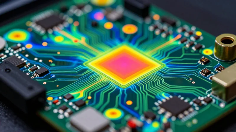
The Role of Ceramics in High-Power Electronics
Ceramic substrates provide a critical advantage over traditional organic materials (such as FR-4) by combining high thermal conductivity with excellent electrical insulation. In high-power applications, these substrates serve as the primary thermal path for heat generated by semiconductors, ensuring long-term reliability by mitigating the risks of thermal runaway and mechanical fatigue caused by coefficient of thermal expansion (CTE) mismatches.
Comparative Thermal Properties of Substrate Materials
| Material | Thermal Conductivity (W/mK) | CTE (ppm/°C) | Application Focus |
|---|---|---|---|
| FR-4 | 0.2 - 0.4 | 14 - 17 | Low-power control logic |
| Al2O3 (Alumina) | 20 - 30 | 7.0 - 8.0 | General power modules |
| AlN (Aluminum Nitride) | 170 - 230 | 4.5 | High-wattage density/RF |
DFM Considerations for AlN vs. Alumina
When integrating ceramic substrates into assembly workflows, engineers must account for the inherent material brittleness of ceramics. DFM rules prioritize stress reduction during the soldering and clamping processes, as these materials lack the mechanical flex common in organic substrates.
- Why is CTE matching vital for ceramic PCBs?
Ceramics are rigid and do not deform under stress. If the substrate material does not match the CTE of the mounted silicon power devices, thermal cycling will lead to rapid solder joint fatigue and potential cracking of the substrate itself. - What is the primary constraint of AlN compared to Al2O3?
While AlN offers exceptional thermal conductivity, it is significantly more expensive and susceptible to moisture degradation if the surface metallization is compromised, necessitating strict environmental controls during assembly. - How should metallization be approached for thermal performance?
For high-performance applications, Direct Bonded Copper (DBC) is preferred over thick-film technology. The increased copper thickness provided by DBC lowers electrical resistance and enhances lateral heat spreading across the substrate surface.
Core DFM Rules for Ceramic PCB Geometry
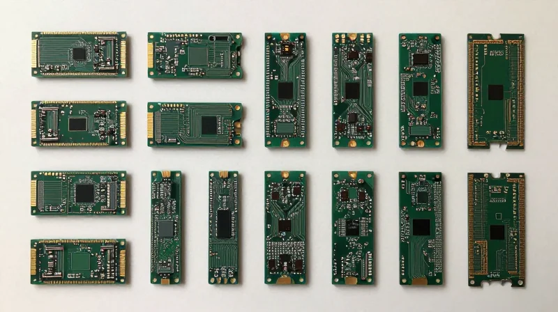
Ceramic substrates, such as Aluminum Nitride (AlN) and Alumina (Al2O3), are brittle and sensitive to mechanical stress compared to organic FR-4 boards. Establishing rigorous geometric design rules is essential to prevent micro-cracking and delamination during machining, assembly, and thermal cycling. Engineers must prioritize uniform feature distribution and stress-relieving mechanical geometries to maintain the integrity of these high-performance materials.
Critical Clearance and Spacing Parameters
| Feature Type | Minimum Clearance Rule | Manufacturing Rationale |
|---|---|---|
| Edge-to-Copper | 0.50 mm | Prevents lateral cracking and electrical arcing during laser/dicing. |
| Hole-to-Hole | 2.0x Wall Thickness | Maintains structural rigidity between through-hole features. |
| Hole-to-Edge | 1.50 mm | Reduces tensile stress concentrations at board corners. |
Panelization and Micro-cracking Prevention
Panelization of ceramic PCBs is prone to fractures if not handled with precision. Avoid 'mouse bites' or perforated tabs that generate excessive vibration or shear force. Instead, utilize laser-scored breakaway tabs or solid frame rails with routing that avoids sharp 90-degree inner corners. High-stress concentration points should be mitigated with rounded radii, as ceramic materials lack the elasticity to compensate for abrupt structural transitions.
Frequently Asked Questions
- Why is the 1.5mm hole-to-edge rule critical for ceramics?
Ceramics exhibit low fracture toughness. Placing holes closer to the edge introduces high stress concentration factors, which leads to crack propagation during the mechanical singulation or thermal shock phases of production. - How does substrate thickness influence hole aspect ratio?
Due to the hardness of AlN and Al2O3, laser drilling is often required. Keep aspect ratios below 3:1 to ensure uniform wall metallization and prevent plating voids in deep vias. - Can I use standard CNC routing for ceramic boards?
No, traditional mechanical routing induces localized vibrations and micro-cracking. Laser singulation or diamond-saw dicing is the industry standard for maintaining edge quality and structural reliability.
Advanced Metalization Techniques: DPC vs. DBC
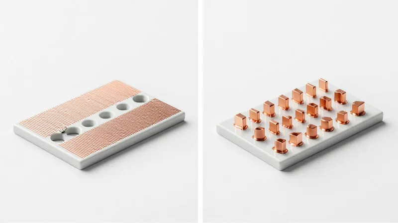
DPC vs. DBC: Performance and Manufacturing Paradigms
Selecting between Direct Plated Copper (DPC) and Direct Bonded Copper (DBC) hinges on balancing fine-line resolution requirements with thermal cycling reliability. DPC utilizes thin-film sputtering and electroplating to achieve precise pattern geometries, whereas DBC employs a high-temperature eutectic bonding process to create a robust, thick-copper interface suited for high-current applications.
| Feature | Direct Plated Copper (DPC) | Direct Bonded Copper (DBC) |
|---|---|---|
| Copper Thickness | 10um - 100um | 100um - 500um |
| Minimum Line Width | 30um - 50um | 150um - 200um |
| Bonding Method | Sputtering/Plating | Eutectic Brazing/Bonding |
| Thermal Conductivity | Moderate | Excellent (High Volume) |
Critical DFM Considerations for Ceramic Metallization
DPC technology is inherently better for high-density interconnects (HDI) where thermal resistance must be balanced against spatial constraints. Conversely, DBC is the industry standard for high-power modules where CTE (Coefficient of Thermal Expansion) mismatch between copper and ceramic poses a fatigue risk during extended thermal cycling. Design engineers must account for the thicker copper edge profiles of DBC, which require larger clearance margins to prevent dielectric breakdown under high-voltage bias.
- Which technology offers superior bonding strength?
DBC generally provides superior bond strength due to the formation of a copper-oxygen eutectic layer that fuses to the ceramic substrate, making it more resilient to mechanical shock and rapid thermal cycling. - Is DPC suitable for high-frequency RF designs?
Yes, DPC is the preferred choice for RF and fine-pitch applications because the plating process allows for significantly tighter tolerance control and smoother copper surface topography compared to the rougher surface of traditional DBC. - How does metallization choice impact DFM clearance rules?
DBC requires larger edge-to-copper clearances compared to DPC to accommodate copper etching limitations and potential burrs inherent in the thick-film bonding process.
Surface Finish Strategies for LED Wire Bonding
Surface finish selection for LED wire bonding must balance metallurgical compatibility, wire loop geometry requirements, and the thermal constraints of ceramic substrates like AlN or Al2O3. In high-power LED assemblies, the finish serves as the critical interface for the gold (Au) or aluminum (Al) wire bonds, requiring a high degree of surface planarity and oxidation resistance to ensure consistent intermetallic compound formation.
Comparative Analysis of Surface Finishes
| Surface Finish | Wire Bond Compatibility | Corrosion Resistance | Cost Profile |
|---|---|---|---|
| ENIG | Excellent (Gold) | High | Moderate |
| ENEPIG | Superior (Universal) | Very High | High |
| Immersion Ag | Good (Requires flux) | Low (Tarnishing) | Low |
Technical Considerations for High-Power LEDs
- Why is ENEPIG preferred over ENIG for high-reliability LEDs?
ENEPIG (Electroless Nickel Electroless Palladium Immersion Gold) introduces a palladium layer that prevents the 'black pad' syndrome and provides a more robust barrier against nickel diffusion, ensuring long-term bond integrity under high-heat cycling. - How does surface planarity affect wire bonding performance?
Ceramic substrates require high planarity to maintain consistent capillary force during ultrasonic bonding. Excessive surface roughness or uneven plating thickness leads to variable bond deformation and potential cratering on thin-film ceramic copper pads. - What are the risks of Silver (Ag) finishes in LED applications?
While Silver provides excellent conductivity, it is prone to oxidation and sulfurization, which can degrade wire bond reliability if the ceramic PCB is stored in uncontrolled environments prior to assembly.
For DFM compliance, designers should specify a nickel thickness of 3-6μm for structural stability and a gold thickness of at least 0.05-0.1μm for wire bonding. When dealing with AlN substrates, ensure that the chosen finish is compatible with the underlying metallization (DPC or DBC) to avoid interface delamination during the high-temperature bond process.
Overcoming Coefficient of Thermal Expansion (CTE) Mismatches
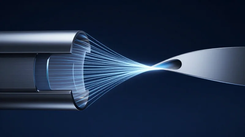
Managing CTE Mismatch in Ceramic Assemblies
CTE mismatch occurs when materials with differing thermal expansion rates are bonded together, creating significant shear stresses at the interface during thermal cycling. For ceramic PCBs, the rigid nature of substrates like Alumina (Al2O3) or Aluminum Nitride (AlN) compared to metallic heat sinks and LED dies necessitates deliberate DFM strategies to avoid solder joint fatigue, delamination, or ceramic cracking.
Mitigation Material Comparison
| Material/Interface | CTE (ppm/°C) | Mitigation Strategy |
|---|---|---|
| Alumina Ceramic | 6.5 - 7.5 | Use CTE-matched Cu-Mo alloys |
| Aluminum Nitride | 4.5 - 5.0 | Apply ductile thermal interface materials |
| Copper Heat Sink | 16.5 - 17.0 | Implement stress-relieving interlayers |
| LED Die (Sapphire/GaN) | 5.0 - 7.0 | Optimized eutectic die attach |
Design Best Practices
- Use Compliant Interlayers
Incorporate low-modulus adhesives or soft solder alloys (such as Indium-based solders) to absorb mechanical strain between the rigid ceramic and the base plate. - Symmetry in Layout
Distribute copper traces and heat-generating components symmetrically to ensure uniform thermal expansion, preventing warping and localized stress concentrations. - Thermal Buffer Zones
Avoid placing high-power components near the ceramic edges where edge-loading and mechanical weakness are most prevalent.
Frequently Asked Questions
- How does ceramic thickness affect CTE stress?
Thicker ceramic substrates increase total internal stress during thermal excursions; thinner substrates offer greater flexibility at the cost of potential bowing. - Is DBC or DPC better for minimizing CTE stress?
DBC (Direct Bonded Copper) involves high-temperature processes that introduce significant residual stress, whereas DPC (Direct Plated Copper) typically offers a lower thermal budget, resulting in less inherent stress post-fabrication.
Inspection Standards and Quality Control
Advanced Inspection Methodologies for Ceramic Substrates
Given the brittle nature of ceramic materials like AlN and Al2O3, standard optical inspection is insufficient for detecting internal delamination or micro-voiding. High-performance assembly requires a multi-layered inspection strategy that integrates non-destructive testing with precise thermal validation to ensure the reliability of the copper-ceramic bond.
| Method | Primary Application | Detection Capability |
|---|---|---|
| X-Ray Inspection (2D/3D) | Solder Joint Integrity | Voids, bridging, and alignment shifts |
| SAM (Scanning Acoustic Microscopy) | Interface Bonding | Sub-surface delamination and cracks |
| Thermal Imaging | Heat Dissipation | Hot spots and thermal path continuity |
Key Quality Control Metrics
- Void Percentage Thresholds
For high-power ceramic PCBs, solder joint voiding should be maintained below 10-15% of the total pad area to prevent localized thermal bottlenecks. - Bond Strength Consistency
Destructive shear testing on coupon samples is required for every production batch to verify the DBC/DPC metalization adhesion forces meet the minimum N/mm2 specification. - CTE Stress Verification
Post-assembly thermal cycling (typically -55°C to +125°C) is mandatory to ensure that the assembly can withstand stresses arising from coefficient of thermal expansion (CTE) mismatches.
Best Practices for Destructive and Non-Destructive Testing
While non-destructive techniques like Automated Optical Inspection (AOI) capture assembly placement errors, they cannot reveal internal metallurgical fatigue. Implementing cross-sectional analysis on sample boards allows engineering teams to inspect the integrity of the ceramic-metal interface under a scanning electron microscope (SEM). This provides granular data regarding the thickness of the reaction layer, ensuring that chemical processing during DPC or DBC plating has not compromised the substrate's mechanical structural integrity.
Optimizing Assembly and Reflow Profiles
Managing Thermal Mass and Heat Soaking
Ceramic substrates, such as Alumina (Al2O3) and Aluminum Nitride (AlN), exhibit significantly higher thermal mass than traditional FR-4 materials. Consequently, they function as heat sinks that dissipate energy away from the solder joints during the reflow process. To ensure complete solder wetting, reflow profiles must be extended in the soak zone to allow the entire substrate to reach a uniform equilibrium temperature before entering the spike phase.
| Parameter | FR-4 Guideline | Ceramic PCB Guideline |
|---|---|---|
| Preheat Rate | 1.0-3.0°C/s | 0.5-1.5°C/s |
| Soak Time | 60-90s | 120-180s |
| Peak Temp | 235-245°C | 245-260°C |
Solder Paste Selection and Reflow Optimization
Choosing the right alloy is critical for ceramic assemblies. High-melting-point lead-free alloys, such as SAC305 or specialized high-reliability alloys with bismuth or antimony additions, are preferred to manage the CTE mismatch. Due to the high heat absorption of ceramics, nitrogen (N2) atmosphere reflow is strongly recommended to broaden the process window and reduce oxidation during the extended soak times required for proper wetting.
Frequently Asked Questions
- Why is the soak zone longer for ceramics?
Ceramics have high thermal mass; a longer soak ensures that components and pads reach the target temperature simultaneously, preventing cold solder joints. - Should I use Nitrogen for reflow?
Yes. Using a Nitrogen atmosphere reduces surface tension and oxidation, which significantly improves wetting on high-thermal-mass ceramic surfaces. - Does the ramp-up rate affect reliability?
Excessive ramp rates cause localized thermal shock, which can lead to micro-cracking in the ceramic substrate or brittle intermetallic compounds at the joint.
Cost-Effective Scaling for High-Volume LED Manufacturing
Maximizing Panel Utilization and Throughput
The most significant cost driver in ceramic PCB manufacturing is the panel size. Because ceramic substrates like Aluminum Nitride (AlN) or Alumina (Al2O3) are brittle and expensive, maximizing nesting efficiency is critical. Design for Manufacturing (DFM) rules should prioritize tight component spacing and common-rail routing to reduce the amount of waste material generated per panel. By shifting from individual board fabrication to high-density panelized arrays, manufacturers can drastically lower the cost-per-unit by reducing handling cycles and setup times.
Strategies for Scrap Reduction
| Failure Mode | Primary Root Cause | Cost-Saving Mitigation |
|---|---|---|
| Substrate Cracking | Excessive stress from singulation | Laser ablation or precision diamond sawing |
| Solder Voids | Incompatible reflow profile | Vacuum reflow optimization |
| CTE Mismatch Failure | Poor material coupling | Matching CTE of substrate and chip carrier |
Frequently Asked Questions on Scaling Ceramic Assemblies
- How does panelization impact long-term costs?
Increased panel density reduces the number of panels processed through the assembly line, decreasing machine idle time, reducing stencil wear, and lowering energy consumption per LED package. - Can I use standard FR4 fabrication equipment for ceramic PCBs?
While some assembly steps are similar, ceramic requires specialized handling and different singulation tools to prevent chipping, which can cause field failures and lead to higher long-term warranty costs. - What is the role of automated optical inspection (AOI) in cost control?
AOI implemented mid-process prevents value-add on defective units; catching a printing error on a ceramic panel before component placement saves both the high cost of the LED die and the processing time.
Successfully integrating ceramic PCBs into your high-power LED architecture requires precision at every stage of the design-to-assembly lifecycle. By adhering to these DFM principles, you can significantly reduce failure rates and improve product thermal performance. Ready to optimize your next project? Contact our engineering team today to discuss your specific substrate requirements.
