
In the high-stakes world of industrial automation, an RFID reader is only as good as its underlying PCB design. Poor signal integrity or electromagnetic interference can turn a high-read-range system into a liability. This guide provides the technical roadmap for engineers to implement Design for Manufacturing (DFM) principles that ensure reliability, performance, and manufacturability in every RFID project.
The Critical Role of DFM in RFID Systems

Beyond Assembly: The RF Perspective
In standard electronics, DFM often focuses on component placement speed and solder joint integrity. In industrial RFID, however, DFM is inextricably linked to RF performance. A PCB designed without manufacturing constraints in mind may suffer from parasitic capacitance, impedance discontinuities, or trace length variations that degrade reading sensitivity and increase interference susceptibility.
Critical DFM Parameters for RFID Reliability
| Design Factor | Manufacturing Impact | RFID Performance Consequence |
|---|---|---|
| Stack-up Symmetry | Warpage reduction during reflow | Stabilized dielectric constants for antenna matching |
| Trace Tolerance | Etching consistency | Controlled impedance for RF signal integrity |
| Via Placement | Drill alignment and plating | Reduced ground bounce and EMI emissions |
Frequently Asked Questions
- Why is board stack-up critical in RFID?
The stack-up defines the reference planes for high-frequency signals. Improper layer construction leads to impedance mismatch, causing signal reflections that reduce read range and data accuracy. - Can DFM reduce electromagnetic interference (EMI)?
Yes. By optimizing via stitch patterns and decoupling capacitor placement through DFM analysis, designers can minimize current loops, significantly lowering noise floors that would otherwise desensitize the RFID receiver. - Does component tolerance affect antenna tuning?
Absolutely. Using components with tight tolerances (e.g., 0.1% for matching circuits) during the DFM process ensures that the resonant frequency remains within the target band across thousands of mass-produced units.
Optimal Layer Stack-up Configurations
Selecting the Optimal Layer Count
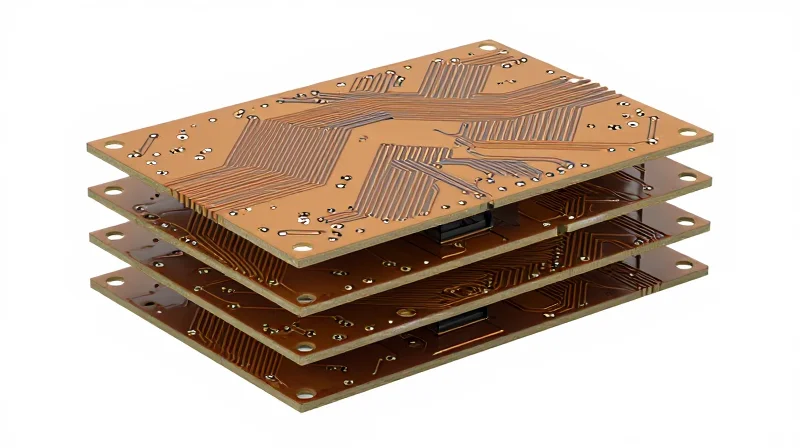
For industrial RFID reader assemblies, a minimum of four layers is standard practice. While two-layer designs may suffice for simple digital logic, they are insufficient for the sensitive RF signal conditioning and noise isolation required for consistent RFID performance in harsh industrial environments.
| Layer Count | Best Use Case | Performance Impact |
|---|---|---|
| 4-Layer | Basic RFID reader modules | Balanced cost and signal integrity. |
| 6-Layer | Complex layouts with MCU + RF | Superior isolation and impedance control. |
| 8+ Layer | High-density industrial gateways | Advanced noise immunity and shielding. |
Core Principles for RF Signal Isolation
Effective isolation relies on proper reference plane allocation. High-speed digital signals and sensitive analog RF traces must be kept physically separate and returned to the ground plane via dedicated paths to prevent cross-talk and harmonic interference.
- Why is the ground plane placement critical?
A solid ground plane immediately adjacent to the signal layer provides a controlled return path, minimizing loop area and reducing the electromagnetic signature of the PCB. - How do you manage RF/Digital coupling?
Implement vertical isolation by placing high-speed digital signals on inner layers sandwiched between ground planes, keeping RF circuitry on outer layers to facilitate antenna connectivity. - What is the role of stitching vias?
Stitching vias along the perimeter of the RF trace area creates a Faraday cage effect, containing signal leakage and preventing board-edge radiation.
DFM Best Practices for Stack-Up Reliability
Symmetry is the foundation of DFM. Always design your stack-up to be symmetrical regarding copper thickness and dielectric materials to minimize board warping during reflow soldering. For industrial applications, specify controlled impedance and ensure the pre-preg selection accounts for both thermal expansion coefficients and the required RF permittivity.
Precision Impedance Matching for Maximum Power Transfer
Precision Impedance Matching for Maximum Power Transfer
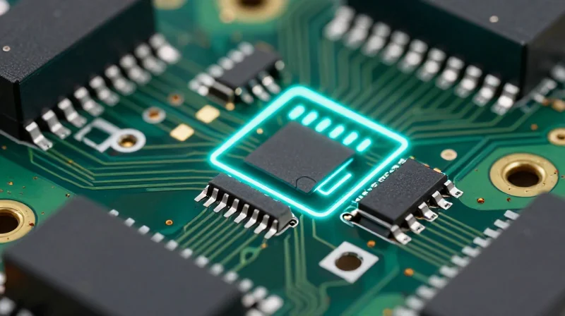
In RFID reader design, the interface between the transceiver IC and the antenna represents a critical point of potential signal degradation. To achieve maximum power transfer, the transmission line must be meticulously matched to 50 ohms. Even minor deviations in trace width, copper thickness, or substrate dielectric constant can induce impedance discontinuities, leading to signal reflection (return loss) that severely curtails the effective read range of the industrial RFID system.
Technical Strategies for 50-Ohm Trace Consistency
Maintaining a stable characteristic impedance requires a unified approach combining precise geometry, controlled substrate properties, and manufacturing collaboration. Engineers must specify strict tolerances for trace dimensions to account for the etching process variations inherent in PCB manufacturing.
| Parameter | Influence on Impedance | Design Mitigation Strategy |
|---|---|---|
| Trace Width | Inverse proportional | Specify +/- 10% tolerance on critical RF traces |
| Dielectric Thickness | Direct proportional | Use material with stable Er over frequency/temp |
| Copper Weight | Direct proportional | Maintain consistent plating targets for uniformity |
Common Impedance Matching Challenges
- How does Vias-in-path impact impedance?
Vias act as inductive discontinuities. When transitioning between layers, use stitch grounding vias in close proximity to the RF signal path to maintain a low-impedance return current loop. - Why is the solder mask problematic?
The presence of solder mask over an RF trace increases the effective dielectric constant, causing the impedance to drop. Ensure that critical RF transmission lines remain clear of solder mask whenever possible. - What is the role of TDR testing?
Time Domain Reflectometry (TDR) is the primary manufacturing verification tool used to locate impedance mismatches along a transmission line, allowing for real-time validation of the DFM design intent.
High-Frequency Component Placement Best Practices
In industrial RFID applications, the physical arrangement of components—specifically RF-critical ICs, matching networks, and decoupling capacitors—dictates the performance limits of the reader. Poor placement introduces unwanted parasitic capacitance and inductance, which can shift resonant frequencies and compromise the sensitivity of the RF front-end.
Strategic Grouping and Routing Rules
To maintain a robust signal path, engineers must prioritize proximity and loop minimization. Components belonging to the RF signal chain should be grouped tightly to minimize trace length, thereby reducing the influence of trace-induced inductance and parasitic coupling to neighboring high-speed digital lines.
| Component Type | Placement Priority | Design Constraint |
|---|---|---|
| Matching Network | Highest | Place as close as possible to the antenna port to prevent signal reflections. |
| Decoupling Caps | High | Place nearest to the IC power pins to minimize current loop area. |
| Digital Logic | Medium | Physically isolate from RF front-end to reduce EMI coupling. |
Addressing Common Placement Challenges
- How do I minimize parasitic inductance in the matching network?
Use the shortest possible traces between components and the antenna port. Avoid vias in the critical signal path, as they introduce discontinuous impedance and inductive spikes. - Should I group decoupling capacitors differently for UHF vs HF?
Yes. While both require close proximity to IC pins, UHF readers demand capacitors with low Equivalent Series Inductance (ESL) placed in a shunt configuration to provide a low-impedance path to ground at higher harmonic frequencies. - How does component orientation affect EMI susceptibility?
Orient inductors perpendicularly to each other to minimize magnetic field coupling. Avoid placing sensitive analog RF lines parallel to high-speed digital buses to prevent cross-talk.
Ultimately, a 'DFM-first' approach requires verifying the placement of components against electromagnetic simulation results. Even minor shifts in component placement can result in significant deviations from the target impedance, potentially leading to costly re-spins in industrial production environments.
Advanced Grounding and Shielding Techniques
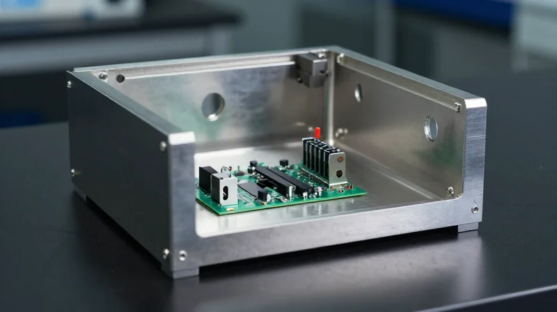
In industrial RFID applications, the PCB serves as both an antenna environment and a high-speed digital processor. To prevent coupling between the noisy digital switching environment and the sensitive RF front-end, designers must implement a multi-tiered approach to grounding and containment. Failure to control return current paths often leads to excessive EMI emissions and receiver desensitization.
Optimizing Ground via Stitching and Impedance Control
Vias are not merely mechanical connections; they are high-frequency impedance discontinuities. For RFID reader PCBs, employing a dense 'via fence' or 'via stitching' strategy is essential. By placing ground vias along the perimeter of RF transmission lines at intervals significantly smaller than one-tenth of the signal's wavelength, you can effectively suppress lateral electromagnetic wave propagation and minimize radiation from board edges.
| Technique | Primary Benefit | Design Rule |
|---|---|---|
| Via Stitching | Edge radiation reduction | Spacing < 1/10 wavelength |
| Guard Traces | Crosstalk suppression | Ground via every 5mm |
| Split Planes | Noise isolation | Maintain bridge continuity |
Physical Shielding Strategies
While board-level grounding is foundational, physical shielding is often required to meet FCC or ETSI emission masks. Implementing surface-mount shield cans provides a Faraday cage effect around high-gain RF components. When utilizing these cans, it is imperative to ensure a low-impedance connection to the reference ground plane using multiple peripheral pads. Poor contact can turn the shield into a parasitic radiator, potentially worsening EMC performance.
Frequently Asked Questions
- Should I use a split ground plane for RF and digital circuits?
Generally, a unified ground plane is preferred. If you must use split planes to isolate noise, you must bridge them at the point of signal transition to prevent large, uncontrolled return current loops. - How do guard traces improve performance?
Guard traces provide a low-impedance path to ground for capacitive coupling. They work best when tied to the primary ground plane at frequent intervals to prevent the guard trace itself from becoming an antenna.
Mitigating Signal Interference in Crowded Environments
Strategies for Mitigating Signal Interference
In high-density industrial deployments, RFID reader PCBs are constantly subjected to electromagnetic interference (EMI) from motors, VFDs, and adjacent wireless equipment. Robust performance relies on a multi-layered approach involving strategic component isolation, differential signaling, and rigorous decoupling methodologies to maintain signal integrity.
Optimizing Decoupling Capacitor Placement
Decoupling capacitors are critical for providing low-impedance paths for high-frequency noise. To maximize effectiveness, capacitors must be placed as close as possible to the IC power pins, with the smallest value capacitor closest to the pad to minimize parasitic loop inductance. Utilizing a multi-capacitor decoupling network provides a wider frequency range of noise suppression.
| Capacitor Type | Placement Strategy | Primary Function |
|---|---|---|
| Bulk (10µF+) | Near power entry point | Low-frequency energy storage |
| Mid-range (0.1µF) | Near IC supply pins | General transient suppression |
| High-freq (10nF/1nF) | Directly at device pads | High-speed switching noise rejection |
Crosstalk and EMI Mitigation Best Practices
- How can I prevent crosstalk on high-speed traces?
Adhere to the '3W' rule—spacing traces at three times their width—and utilize differential pair routing to ensure that electromagnetic fields cancel each other out effectively. - Why is board-level shielding necessary?
Physical metal cans over sensitive RF front-end circuitry provide critical Faraday cage protection, preventing board-level components from acting as unintended antennas for industrial noise. - What is the role of the ground plane in noise reduction?
A solid, uninterrupted ground plane provides the lowest return path impedance, which is essential for minimizing loop area—the primary driver of radiated EMI.
Implementation Code Example: Grounding Via Pattern
/* Design Rule for Via Stitching around RF sensitive areas */
const STITCHING_VIA_RULE = {
  pitch: '2.5mm',
  diameter: '0.3mm',
  net: 'GND',
  layer_constraint: 'All_Layers'
};
// Ensure via fence borders the analog front-end perimeter
DfM Verification: Pre-Production Simulation and Testing

Virtual Prototyping and Simulation
Before committing to physical hardware, RFID reader designs must undergo rigorous virtual validation. Utilizing 3D full-wave electromagnetic (EM) simulators allows engineers to model the antenna-to-PCB interface, identifying impedance mismatches and potential interference hotspots that are often invisible in standard schematic capture.
| Simulation Type | Primary Goal | RFID Impact |
|---|---|---|
| Signal Integrity (SI) | Maintain signal timing and waveform purity. | Prevents data packet loss in high-speed RFID streams. |
| Thermal Analysis | Ensure heat dissipation under peak power. | Prevents frequency drift due to thermal expansion. |
| Electromagnetic (EM) | Model parasitic radiation and coupling. | Increases read range and reduces false triggers. |
Iterative Testing Protocols
Transitioning to physical prototypes requires a structured DfM verification cycle. Rapid prototyping of small-batch PCBA runs allows for real-world verification of simulated findings, ensuring that the manufacturing process does not introduce structural variability that could jeopardize RFID performance.
- How does pre-production simulation reduce costs?
Simulation identifies layout flaws, such as trace impedance errors or thermal hotspots, before costly physical boards are fabricated, avoiding multiple expensive assembly iterations. - Why is field-testing necessary for industrial RFID?
Laboratory conditions rarely replicate the high-interference, metal-dense, and vibration-heavy environments of industrial facilities; field testing validates the PCB against specific ambient noise profiles.
Design Rule Check (DRC) Automation
DRC_Check_List = ['Antenna_Isolation', 'Via_Stitching_Density', 'Clearance_Min', 'Thermal_Relief_Checks']
for check in DRC_Check_List:
    Run_Automated_Validation(check, layer_map=True)
    Log_Violation_Severity('RFID_Design_Constraints')
Robust RFID performance is a direct result of meticulous PCB architecture. By adhering to these DFM best practices, you can minimize production defects and field failures while maximizing your hardware's efficiency. Ready to elevate your hardware design? Contact our engineering team today for a comprehensive design review of your next RFID project.
