
In the high-stakes world of dental diagnostics, equipment reliability is not optional—it is a patient safety imperative. Designing PCBs that manage the intense voltages required for X-ray generation while maintaining high-fidelity imaging is a complex engineering challenge. This guide outlines the essential DFM strategies and stack-up configurations required to eliminate the risk of electrical arcing and failures in sensitive diagnostic hardware.
The Physics of Failure: Arcing in High-Voltage Systems
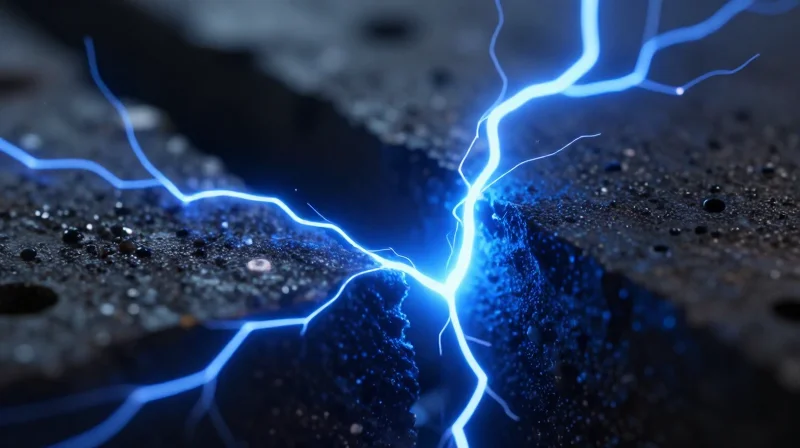
The Mechanics of Electrical Breakdown
In dental X-ray equipment, high-voltage components are susceptible to dielectric breakdown, where the insulating medium—be it air, PCB substrate, or potting compound—fails to withstand the applied electric field. Arcing occurs when the electric field strength exceeds the dielectric strength of the insulator, causing ionized pathways to form. In high-precision medical imaging, even a micro-discharge can compromise image quality or induce permanent hardware degradation.
Creepage vs. Clearance
| Feature | Definition | Primary Failure Path |
|---|---|---|
| Clearance | Shortest distance through air | Ionized air breakdown |
| Creepage | Shortest path along the surface | Surface tracking/contamination |
While clearance is limited by the breakdown of air, creepage is significantly influenced by the Comparative Tracking Index (CTI) of the PCB laminate. Moisture, dust, and ionized particulates can facilitate tracking, creating carbonized conductive paths across the insulator surface over time.
FAQs on Arcing Prevention
- How does PCB surface finish affect arcing?
Rough surface finishes or exposed copper edges create electric field concentrations (corona effect), which lowers the threshold for initial ionization and arcing. - Why is potting essential for high-voltage sections?
Potting materials provide a higher dielectric constant than air, effectively suppressing corona discharge and preventing conductive contaminants from reaching sensitive traces. - What role does altitude play in DFM?
As air density decreases with higher altitudes, the dielectric strength of air drops significantly, requiring increased clearance distances to maintain the same insulation integrity.
Defining Strict Creepage and Clearance Limits
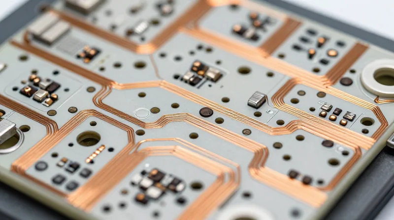
Navigating IEC 60601-1 Compliance
For dental X-ray equipment, compliance with IEC 60601-1 is non-negotiable. Designers must calculate minimum spacing requirements based on the device's rated voltage, pollution degree, and insulation category. Unlike standard consumer electronics, medical-grade high-voltage (HV) circuits require a systematic approach to prevent hazardous discharges, specifically distinguishing between the shortest path across a surface (creepage) and through the air (clearance).
| Parameter | Definition | Key DFM Consideration |
|---|---|---|
| Clearance | Shortest distance through air. | Must account for atmospheric pressure changes. |
| Creepage | Shortest distance across a surface. | Requires CTI (Comparative Tracking Index) material selection. |
Critical Factors for High-Voltage Isolation
- How does Pollution Degree affect design?
Pollution Degree (PD) defines the amount of conductive contamination expected. For dental environments, PD 2 is typically standard, but high-humidity areas require moving to PD 3, which mandates significantly larger creepage distances. - Why is CTI rating important for PCB materials?
The Comparative Tracking Index indicates a material's resistance to surface tracking. Higher CTI materials allow for closer component placement without risking long-term electrical breakdown. - How should slots be used in board layout?
Routing slots between HV and low-voltage traces effectively increases the creepage path without requiring a larger total board size, as the measurement path must travel around the void.
Best Practices for Implementation
Engineers should employ 'keep-out' zones in their EDA software to enforce these limits automatically. It is vital to consider peak operating voltages rather than nominal voltages when calculating distances, as dental X-ray generators often experience significant transients during tube activation. Always verify spacing at the component level, as lead pitch and solder mask openings can inadvertently create shorter paths than the intended PCB traces.
Strategic Stack-Up Configurations for HV Isolation
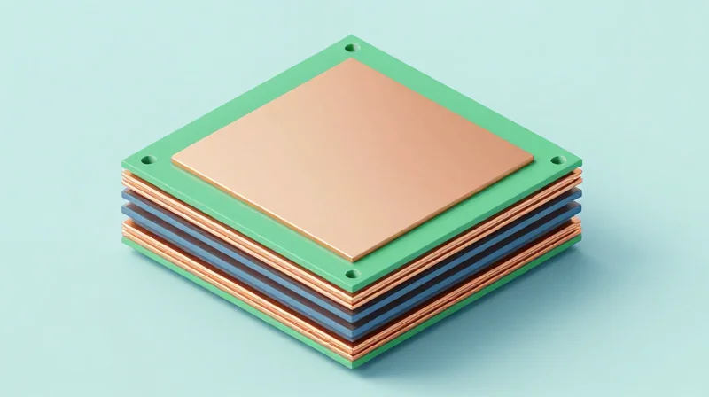
Strategic Stack-Up Configurations for HV Isolation
Achieving robust high-voltage isolation in dental X-ray equipment requires a meticulous approach to layer stack-up design, prioritizing dielectric strength and the mitigation of capacitive coupling between high-voltage traces and sensitive low-voltage control circuitry.
Dielectric Material Selection and Layer Balancing
The primary defense against internal layer-to-layer breakdown is the selection of high-Cti (Comparative Tracking Index) substrates and the calculation of appropriate prepreg thicknesses. To ensure long-term reliability, avoid using thin dielectrics between high-potential layers; instead, utilize symmetric balanced stack-ups that minimize mechanical stress and warpage during the thermal cycling inherent to X-ray generation.
| Stack-up Strategy | Primary Benefit | Critical Implementation |
|---|---|---|
| Symmetric Layering | Mechanical Stability | Align copper weights on top/bottom layers |
| Increased Prepreg Thickness | Higher Dielectric Strength | Verify resin content for high-voltage integrity |
| Embedded HV Isolation | Reduced Parasitic Capacitance | Implement keep-out zones on adjacent internal layers |
Mitigating Parasitic Capacitance
High-voltage switching in dental X-ray power supplies generates significant dV/dt, which can inject noise into control circuitry through parasitic capacitance between PCB layers. Strategic placement of ground shields between HV and low-voltage planes is critical.
- How does layer stack-up affect EMI?
Improper stack-ups can lead to capacitive coupling between primary HV traces and signal planes, causing ground bounce and signal interference. - Why avoid thin core materials in HV designs?
Thin cores increase the electric field gradient across the dielectric, significantly raising the probability of localized insulation breakdown under high-voltage stress. - What role does copper balancing play?
Copper balancing prevents PCB warping during the reflow process, which ensures that prepreg thickness remains uniform, maintaining consistent isolation distances across the board.
Advanced PCB Material Selection for HV Applications
Optimizing Substrate Material for High-Voltage Reliability
In dental X-ray applications, standard FR-4 often falls short due to insufficient Comparative Tracking Index (CTI) ratings. When subjected to the high-voltage potential required for tube heads, organic resins can undergo carbonization, creating conductive paths that lead to catastrophic device failure. Engineers must prioritize high-CTI substrates or specialized ceramics that offer superior resistance to electrical tracking and moisture absorption.
Material Comparison for HV Performance
| Material Type | Typical CTI (V) | HV Suitability | Thermal Conductivity |
|---|---|---|---|
| Standard FR-4 | 175-225 | Poor | Low |
| High-CTI FR-4 | 600+ | Good | Low |
| Polyimide | 250-300 | Moderate | Medium |
| Ceramic (Alumina) | 800+ | Excellent | High |
Frequently Asked Questions
- Why is CTI value critical in dental X-ray PCBs?
The CTI represents the voltage threshold at which a material fails due to the formation of conductive tracking. A higher CTI rating prevents short circuits across the PCB surface in the presence of contaminants or humidity. - Is standard FR-4 ever acceptable for HV?
While standard FR-4 is cost-effective, it is generally unsuitable for high-voltage DC paths in medical devices. If used, extreme design margins for creepage are required to compensate for its low tracking resistance. - When should I consider ceramic substrates?
Ceramic substrates are ideal for extreme miniaturization where spacing requirements (creepage/clearance) cannot be met with polymer-based boards, as they offer superior electrical isolation and thermal stability.
Layout Techniques to Prevent Arcing
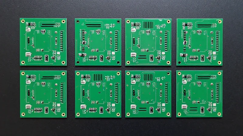
Implementing Geometric Isolation Features
To mitigate surface tracking and arcing, designers must manipulate the PCB substrate geometry beyond simple clearance distances. Incorporating slots or V-grooves between high-potential traces increases the surface creepage path length significantly, as voltage must traverse the air gap or the contour of the material rather than following a direct line. This approach is highly effective in dense dental imaging boards where space is at a premium.
| Feature | Mechanism | Primary Application |
|---|---|---|
| Milled Slots | Increases creepage length through air | High-voltage terminal isolation |
| V-Grooves | Disrupts conductive path tracking | Polluted or high-humidity environments |
| Conformal Coating | Increases dielectric strength of surface | Dense component proximity |
Strategic Material and Barrier Application
Conformal coatings serve as the final line of defense against atmospheric arcing, particularly in dental environments prone to high humidity. Utilizing high-dielectric strength silicone or acrylic resins prevents ionized gas paths from forming between conductors. Designers should ensure that coatings are applied uniformly and that they maintain adhesion to the board surface, as gaps in the material can lead to localized corona discharges.
Frequently Asked Questions on Arcing Mitigation
- How do slots improve isolation compared to surface paths?
Slots force the creepage path to follow the contours of the PCB material or jump through the air, significantly increasing the effective distance required for electrical breakdown. - Why is conformal coating necessary if clearance is already met?
Even with sufficient clearance, contaminants or moisture can lower the breakdown voltage; conformal coating seals the surface to provide consistent dielectric insulation regardless of environmental changes. - Are there specific design rules for slot widths?
Yes, standard manufacturing tolerances typically require a minimum slot width (e.g., 1.5mm to 2mm) to ensure physical robustness and ease of cleaning during the fabrication process.
Minimizing Electromagnetic Interference (EMI) in Imaging Hardware
Strategic Partitioning and Signal Isolation
The fundamental defense against EMI in dental imaging hardware is the absolute physical and electrical separation of the high-voltage (HV) generation circuitry from sensitive analog front-end (AFE) components. By utilizing distinct ground planes—a quiet analog ground for the sensor and a chassis/return ground for the power stages—you prevent high-frequency current loops from inducing noise into the low-voltage signal chain. Bridging these domains should only occur at a single, well-defined point, often via a ferrite bead or a low-inductance connection to ensure potential equalization without creating ground loops.
EMI Mitigation Strategy Comparison
| Strategy | Mechanism | Primary Benefit |
|---|---|---|
| Differential Signaling | Balanced transmission | High common-mode noise rejection |
| Guard Traces | Grounded copper paths | Reduction of capacitive coupling |
| Faraday Shielding | Enclosure integration | External RF interference blocking |
Common EMI Challenges and Solutions
- How can I prevent switching noise from the HV power supply from affecting the sensor data?
Utilize dedicated local decoupling capacitors with low ESR values directly at the IC pins and implement soft-switching topologies to reduce the high dV/dt rates associated with power transitions. - What role does trace routing play in EMI reduction?
Minimize loop areas by routing critical return paths directly underneath signal traces. Avoid crossing split planes, as this forces return currents to take unpredictable, inductive paths that act as antennas. - Are via fences necessary for high-frequency isolation?
Yes; implementing a via fence—a series of closely spaced, grounded vias along the perimeter of high-speed traces—effectively contains electromagnetic fields and prevents board-edge radiation.
For designers, the goal remains minimizing radiated emissions through optimized routing and shielding. Always prioritize a low-impedance ground reference and ensure that the return path for every high-speed signal is as short as possible to maintain signal integrity throughout the imaging process.
DFM Verification: Simulation and Testing Protocols
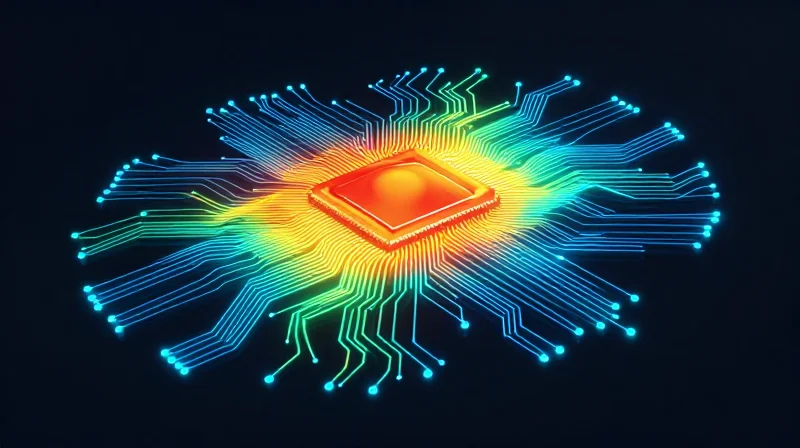
Virtual Verification: FEA and Field Analysis
Before committing to physical fabrication, Finite Element Analysis (FEA) is essential to model the electrostatic potential across the PCB layout. By simulating the electric field intensity, engineers can identify high-stress points where arcing or corona discharge is likely to occur, particularly near sharp copper edges or vias. Modern simulation suites allow for the visualization of field lines, enabling iterative refinements to trace geometries and clearance gaps until field strength remains below the dielectric breakdown threshold of the substrate and coating materials.
Protocols for Destructive and Stress Testing
Validation goes beyond digital models; physical stress testing mimics the harsh lifecycle of dental imaging hardware. These protocols ensure that boards maintain their structural and electrical integrity under thermal cycling, vibration, and peak voltage spikes.
| Test Method | Primary Goal | Pass Criteria |
|---|---|---|
| High-Pot Testing | Verify insulation integrity | No breakdown at 1.5x nominal voltage |
| Thermal Cycling | Test material expansion | No delamination or trace cracking |
| Partial Discharge (PD) | Detect internal voids | Pulse count below industry limit |
Frequently Asked Questions
- Why is Partial Discharge (PD) testing critical for X-ray boards?
PD testing identifies microscopic defects within the insulation system that can gradually degrade over time, leading to catastrophic failure under prolonged high-voltage stress. - How does moisture impact simulation accuracy?
Humidity significantly lowers the effective CTI of the PCB material. Simulations should include worst-case environment factors, such as high-humidity conditions common in dental offices. - Is physical testing necessary if simulations are perfect?
Yes. Simulations cannot fully account for material manufacturing variances or inconsistencies in conformal coating application, making destructive verification a mandatory step for medical compliance.
Supply Chain and Manufacturing Considerations
Selecting the Right Fabricator for High-Reliability Medical Boards
Manufacturing high-voltage circuitry for dental imaging involves challenges that standard PCB houses are often ill-equipped to handle. You must seek partners with specialized experience in high-density interconnect (HDI) processes, strict dielectric strength testing, and compliance with medical certifications such as ISO 13485. A manufacturer's ability to maintain tight tolerances for trace width and copper thickness directly impacts the long-term insulation stability of your high-voltage power supply units.
Critical DFM Fabrication Metrics
| Requirement | Impact on HV Layout | Fabrication Standard |
|---|---|---|
| Dielectric Thickness | Voltage breakdown prevention | Controlled impedance/thickness |
| Copper Plating | Thermal management & current load | Class 3 IPC standards |
| Surface Cleanliness | Elimination of conductive contaminants | Ionic contamination testing |
Supply Chain Resilience and Regulatory Compliance
Maintaining a stable supply chain is paramount for medical devices where even minor component changes can necessitate a costly re-certification process. Establishing early-stage communication with vendors regarding raw material availability (such as specialized high-CTI laminates) ensures that the design remains manufacturable throughout the product lifecycle.
- How do I ensure design continuity if my primary fabricator faces disruptions?
Maintain a 'Golden File' set that includes detailed stack-up specifications, material data sheets, and specific fabrication notes, allowing for rapid transition to a secondary, pre-qualified vendor. - What role does traceability play in high-voltage PCB manufacturing?
Traceability is critical; for medical equipment, every lot of boards must be linked to specific raw material certificates, test reports, and operator logs to satisfy global regulatory auditing requirements. - Should I involve my fabricator during the layout phase?
Yes. Engaging your fabricator during the DFM phase allows for 'Design for Manufacturing' reviews that identify potential etching or lamination bottlenecks before the layout is finalized.
Achieving precision in dental X-ray hardware requires a disciplined approach to PCB layout where high-voltage demands meet medical-grade safety standards. By strictly adhering to these DFM best practices, engineers can ensure both patient safety and superior diagnostic imaging performance. Contact our engineering team today to discuss your next high-voltage project and ensure your design meets global regulatory requirements.
