
In the fast-paced world of modern dentistry, equipment failure isn't just an inconvenience—it's a direct threat to your revenue and patient trust. While the initial cost of premium high-voltage PCB designs might seem higher, the long-term financial impact tells a different story. We explore how advanced engineering reduces the hidden costs of downtime.
The Real Cost of Equipment Downtime in Dental Practices
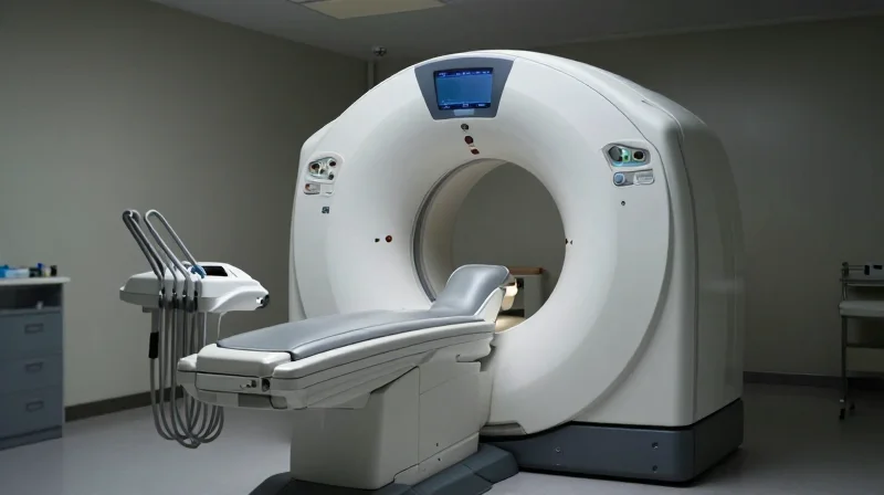
The Financial Impact of Imaging Equipment Failure
Unexpected downtime in a dental practice is not merely an equipment issue; it is a profound revenue drain. When an imaging system—such as a Cone Beam Computed Tomography (CBCT) or digital panoramic unit—goes offline, the practice loses the ability to perform diagnostics, confirm treatment plans, and complete high-value procedures. This creates a cascade effect where overhead costs persist while daily production drops to zero, and patient trust diminishes due to scheduling cancellations.
| Impact Area | Economic Consequence | Operational Ripple Effect |
|---|---|---|
| Direct Revenue | Loss of per-scan billing | Inability to close treatment plans |
| Clinical Efficiency | Overtime for staff rescheduling | Bottlenecks in workflow |
| Patient Retention | Cost of acquiring new patients | Potential loss of long-term loyalty |
Quantifying the Cost of Downtime
Calculating the true cost of downtime requires looking beyond repair bills. Practices must account for 'opportunity cost,' which encompasses the lost time of highly trained clinicians and the administrative labor required to communicate with patients. In high-output clinics, a four-hour outage can result in thousands of dollars of lost production, often far exceeding the price difference between premium, high-voltage-rated components and budget alternatives.
Frequently Asked Questions
- Why are high-voltage PCBs prone to failure?
These boards are exposed to intense thermal stress and frequent power cycling; substandard components fail when they cannot manage these rapid electrical shifts. - How does PCB quality affect ROI?
Premium PCB designs with robust voltage regulation increase Mean Time Between Failures (MTBF), directly extending the life of the imaging unit and reducing emergency service calls. - Is preventative maintenance enough?
Maintenance helps, but it cannot fix inherent weaknesses in circuit design. High-quality electronics provide a fundamental layer of reliability that service visits cannot replicate.
Anatomy of a Failure: Why Standard PCBs Fall Short
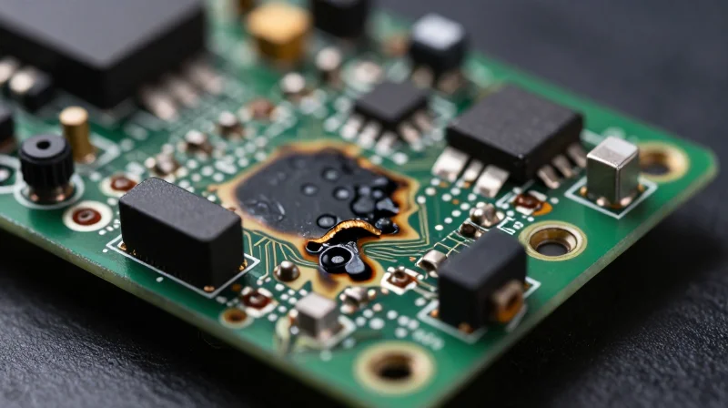
The Thermal Vulnerability of Commodity Electronics
In the demanding environment of dental imaging, standard PCBs are frequently pushed beyond their design thresholds. High-voltage generation creates localized hotspots that standard substrate materials like FR-4 often struggle to dissipate. Over time, these cyclic thermal loads lead to micro-fractures in solder joints and the degradation of trace integrity, ultimately resulting in intermittent system failures that are notoriously difficult to diagnose.
Performance Comparison: Standard vs. Premium High-Voltage PCBs
| Feature | Standard PCB | Premium HV PCB |
|---|---|---|
| Thermal Management | Basic FR-4 (Low Conductivity) | Advanced Ceramics/Metal Core |
| Voltage Isolation | Standard Dielectric Spacing | High-Cti Materials/Guard Traces |
| Fatigue Resistance | Low Cycle Tolerance | Extended Thermal Cycling |
| Mean Time Between Failures | Short (Reactive Maintenance) | Long (Proactive Uptime) |
Common Failure Vectors in Diagnostic Systems
- Why do solder joints fail under high voltage?
Continuous electrical stress combined with thermal expansion mismatch causes solder fatigue, leading to brittle joints that eventually lose electrical continuity. - What role does dielectric breakdown play?
Standard PCB insulating layers may suffer from microscopic carbon tracking when exposed to high voltages, creating short circuits that permanently disable imaging modules. - How does moisture exacerbate the issue?
Dental offices often have high humidity; substandard board coatings allow moisture to bridge critical gaps, causing corona discharge and permanent component damage.
The Engineering Advantage of High-Performance PCBs
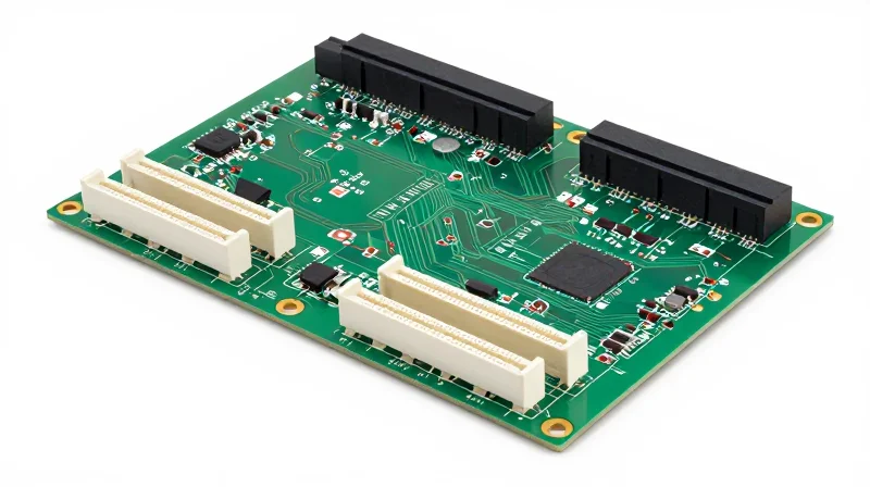
The Engineering Advantage of High-Performance PCBs
Premium high-voltage PCBs are designed specifically to withstand the volatile electrical environments inherent in diagnostic imaging, where consistent power delivery is critical. By transitioning from standard mass-produced boards to high-performance, application-specific designs, manufacturers can mitigate the core triggers of electronic failure, such as dielectric breakdown and conductive path degradation. This engineering approach focuses on the intersection of thermal stability and signal integrity.
Core Pillars of Reliable High-Voltage Design
- Advanced Thermal Management
Utilizing high thermal conductivity substrates and strategic copper pouring allows for rapid dissipation of heat away from critical high-voltage components, preventing the rapid aging of capacitors and semiconductors. - Optimized Dielectric Strength
By selecting materials with higher CTI (Comparative Tracking Index) ratings, boards prevent electrical arcing and surface carbonization under high potential, which are primary causes of catastrophic failure in dental X-ray generators. - Signal Integrity and Layout
Implementing rigorous trace spacing and isolating high-voltage circuits from sensitive logic controllers minimizes EMI-induced errors and prevents cross-talk that leads to intermittent system reboots.
Comparative Reliability: Standard vs. Premium Architectures
| Feature | Standard PCB | Premium High-Voltage PCB |
|---|---|---|
| Dielectric Rating | Basic FR-4 | High CTI/Advanced Ceramic |
| Copper Thickness | Standard 1oz | 2oz to 4oz (Heavy Copper) |
| Thermal Strategy | Passive/Convection | Active Thermal Vias/Heat Spreading |
| Expected MTBF | Moderate | High (Extended 30-50%) |
Ultimately, the shift to high-performance PCBs is a shift in capital expenditure strategy. While the initial investment in premium board design may be higher, the reduction in mid-lifecycle component replacement and the prevention of emergency service calls directly lower the Total Cost of Ownership (TCO) for dental practices.
Signal Integrity and Precision Imaging
The Direct Correlation Between Signal Integrity and Diagnostic Accuracy
In dental imaging, the high-voltage chain is the heartbeat of diagnostic clarity. When signal integrity is compromised by poor PCB design—such as electromagnetic interference (EMI) or signal jitter—the resulting radiographs suffer from loss of contrast, spatial resolution degradation, and unpredictable artifacts. By implementing premium PCB design strategies, engineers create a stable, low-noise environment that allows the detector to capture the highest fidelity data, directly reducing the frequency of diagnostic uncertainty and the resulting requirement for patient re-scans.
Technical Drivers of Precision Imaging
- Controlled Impedance Routing
Ensures that high-frequency signals reach the detector without reflection or distortion, preventing ghosting and blurring effects in the final image. - Advanced Ground Plane Architectures
Provides a clean reference point for sensitive analog-to-digital converters, isolating the high-voltage noise from the fragile image-processing logic. - Material Dielectric Consistency
Uses low-loss materials to maintain signal energy across high-voltage transitions, ensuring that every captured photon translates to an accurate pixel value.
Standard vs. Premium PCB Architecture Comparison
| Feature | Standard PCB Design | Premium HV PCB Design |
|---|---|---|
| EMI Shielding | Basic or non-existent | Integrated copper shielding & localized isolation |
| Thermal Stability | Prone to expansion-induced trace micro-cracks | High-Tg materials ensuring dimensional stability |
| Signal Noise Floor | High susceptibility to noise artifacts | Minimal signal-to-noise ratio for ultra-clear images |
| Imaging Consistency | Occasional diagnostic re-scans required | Reliable, repeatable high-resolution output |
FAQ: Engineering Impact on Clinical Efficiency
- How does signal integrity affect equipment uptime?
High-quality designs prevent the premature degradation of sensitive electronic components, ensuring that the imaging chain remains calibrated and operational for longer periods. - Why do premium PCBs reduce re-scans?
Better signal-to-noise ratios allow for precise imaging even at lower radiation doses, eliminating the need to re-capture images due to motion blur or digital noise artifacts.
Case Study: ROI Analysis in a Large-Scale Dental Group

Implementation and Operational Baseline
A national dental group operating 45 clinics historically faced a recurring failure rate in their intraoral and panoramic imaging units. Standard-grade PCBs, characterized by thin copper traces and subpar dielectric materials, were failing due to the intense thermal cycling inherent in high-voltage dental imaging cycles. By upgrading to a premium high-voltage PCB architecture featuring enhanced thermal dissipation and industrial-grade components, the organization sought to mitigate maintenance overhead.
Quantifiable Impact on Maintenance and Revenue
| Metric | Standard PCB System | Premium PCB Upgrade |
|---|---|---|
| Mean Time Between Failures (MTBF) | 14 months | 42 months |
| Avg. Annual Maintenance Cost per Unit | $2,400 | $650 |
| Avg. Downtime per Failure | 3.5 days | 0.8 days |
Key Findings
- How did the upgrade impact clinical revenue?
By reducing unscheduled downtime from 3.5 days to less than one day per incident, the group recouped an estimated $1.2 million in potential revenue lost to patient rescheduling and machine unavailability over a three-year period. - What was the most significant technical contributor to ROI?
The adoption of high-Tg (glass transition temperature) substrate materials, which prevented substrate delamination under the extreme heat generated during rapid-fire imaging sequences. - Is the initial capital expenditure justified?
Yes; while premium PCB-backed hardware carries a 20% higher upfront cost, the total cost of ownership (TCO) dropped by 55% within 18 months due to the elimination of emergency repair visits.
The transition demonstrates that the hidden ROI of premium PCB designs lies not only in equipment longevity but in the stabilization of the clinical workflow. By investing in resilient electronics, the dental group successfully decoupled their diagnostic imaging availability from the volatility of standard, failure-prone hardware.
Regulatory Compliance and Medical Safety Standards
Engineering Compliance by Design
Regulatory adherence in dental imaging is not merely a post-manufacturing checklist; it is an intrinsic outcome of superior high-voltage PCB engineering. Premium circuit designs incorporate robust isolation barriers, superior dielectric materials, and advanced creepage and clearance management to meet stringent IEC 60601-1 medical electrical equipment standards. By utilizing high-specification PCBs, manufacturers minimize the risk of electromagnetic interference (EMI) and electrical leakage, which are primary failure points in lower-cost, standard-grade components.
Risk Mitigation via Material Selection
| Feature | Standard-Grade PCB | Premium Medical-Grade PCB |
|---|---|---|
| Dielectric Strength | Moderate (Prone to breakdown) | High (Consistent insulation) |
| Thermal Stability | Low (Risk of warping) | High (Maintains structural integrity) |
| Compliance Reliability | Variable (High re-test rate) | Robust (Fast-track certification) |
Simplifying the Path to Certification
For dental OEMs, the choice of PCB substrate and circuit topography directly impacts the speed-to-market. High-performance PCB architectures are designed with pre-validated thermal dissipation and signal shielding paths, drastically reducing the time required for electromagnetic compatibility (EMC) testing. By mitigating these technical risks early in the design cycle, companies avoid costly redesign loops and accelerate regulatory approval.
Common Compliance and Safety FAQs
- How do high-voltage PCBs impact IEC 60601-1 adherence?
Premium designs feature wider trace spacing and high-CTI (Comparative Tracking Index) materials that exceed clearance requirements, reducing the probability of arc faults and ensuring electrical isolation compliance. - Does premium PCB design influence diagnostic safety?
Yes, by maintaining stable signal integrity under high voltage, these boards prevent erratic power fluctuations that could cause imaging artifacts or system lockups, directly enhancing patient safety during scanning. - Can better PCB design reduce long-term compliance maintenance?
Absolutely. By utilizing components rated for harsh medical environments, systems experience less drift and fewer hardware failures, which means fewer physical system modifications that might trigger expensive re-certification cycles.
The Long-Term Impact on Practice Scalability
Scalability Through Uninterrupted Performance
The long-term scalability of a dental practice is fundamentally tethered to the availability of its diagnostic imaging suite. Premium high-voltage PCB architectures serve as the backbone of this availability, mitigating the 'drift' in component performance that typically leads to intermittent equipment failures. By maintaining precise voltage regulation over millions of imaging cycles, these high-end components prevent the systemic operational bottlenecks that occur when hardware requires unscheduled recalibration or repair.
When a practice aims to scale, the cost of downtime scales exponentially. Replacing standard-grade components with high-voltage, mission-critical PCBs reduces the mean time between failures (MTBF), effectively creating a 'stable infrastructure floor' upon which a practice can confidently increase its patient daily throughput without fear of technical insolvency.
Operational Stability: Standard vs. Premium PCB Integration
| Feature | Standard-Grade PCB | Premium High-Voltage PCB |
|---|---|---|
| Failure Rate | Higher frequency after 24 months | Low/Negligible over 60+ months |
| Scalability Impact | Limits throughput due to downtime | Supports 24/7 high-volume throughput |
| Maintenance Cost | High reactive expenditure | Predictable, preventative budget |
| Clinical Throughput | Interrupted by calibration needs | Consistent, stable diagnostic speed |
Strategic Considerations for Long-Term Growth
- How does PCB longevity affect clinic expansion?
Extended equipment life cycles mean capital expenditure is focused on patient services and staff expansion rather than emergency hardware replacements. - Does premium circuitry support faster patient flow?
Yes; by ensuring consistent imaging performance, machines require fewer 'warm-up' cycles and infrequent recalibrations, allowing for tighter appointment scheduling. - What is the primary ROI driver for scaling practices?
The transition from 'repair-centric' operations to 'availability-centric' operations allows for more reliable revenue forecasting and higher patient throughput.
Making the Investment: What to Look for in PCB Quality
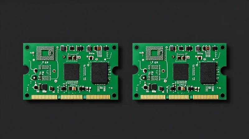
Evaluating PCB Material Integrity for High-Voltage Applications
In dental imaging, premium PCBs must handle high-voltage loads without dielectric breakdown or thermal degradation. When evaluating potential components, prioritize boards that utilize advanced substrate materials like polyimide or high-Tg (glass transition temperature) FR-4. These materials prevent delamination and track erosion, which are primary drivers of sudden clinical downtime.
| Feature | Standard Grade PCB | Premium Medical-Grade PCB |
|---|---|---|
| Dielectric Strength | Basic insulation | Reinforced/High-Voltage rated |
| Thermal Management | Standard copper weight | Heavy copper/Embedded heat sinks |
| Contamination Resistance | Minimal surface treatment | Conformal coated/Hermetic sealing |
Essential Quality Indicators
- How do you verify trace width and spacing?
Ensure manufacturers adhere to IPC-2221 standards for high-voltage spacing to prevent arcing between traces, which is vital for imaging sensors. - What role does surface finish play?
Electroless Nickel Immersion Gold (ENIG) is preferred for medical applications due to its superior solderability and resistance to oxidation in humid clinical environments. - Why is layer stack-up documentation critical?
A well-documented stack-up ensures consistent impedance control, preventing signal noise that could degrade diagnostic image quality over time.
Operational Longevity Through Design
Beyond raw materials, the geometry of the PCB layout dictates the service life of your imaging unit. Look for designs that emphasize 'isolation distance'—the physical space between high-voltage components and sensitive logic circuitry. By minimizing cross-talk and thermal stress, you effectively lower the probability of intermittent faults that lead to expensive, unscheduled technician visits.
Investing in premium high-voltage PCB designs is not merely an equipment upgrade; it is a strategic financial decision that safeguards your practice against the volatility of system failure. By prioritizing component reliability, you ensure operational continuity and a healthier bottom line. Contact our engineering team today to learn how we can optimize your diagnostic hardware for maximum longevity.
