DIY PCB Maker: A Comprehensive Guide to Home Circuit Board Creation
2025.01.12
In our increasingly interconnected world, electronics are the backbone of our daily lives. But what if you could dive deeper and create your own electronic foundations? That's where DIY PCB making comes in. This article empowers you to understand the basics and guides you through the process of creating your own circuit boards at home, connecting your creativity to tangible technology.
Understanding PCB Basics: What is a PCB and Why DIY?
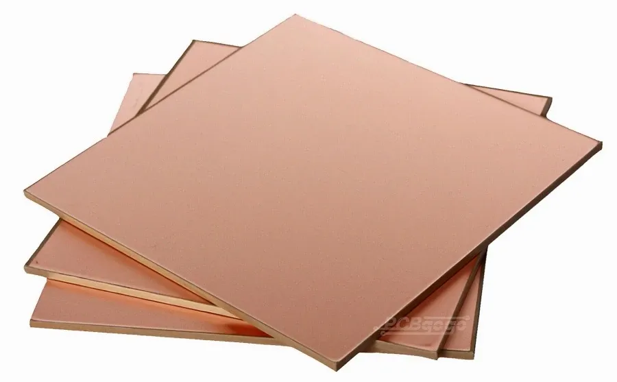
Copper Clad Laminate
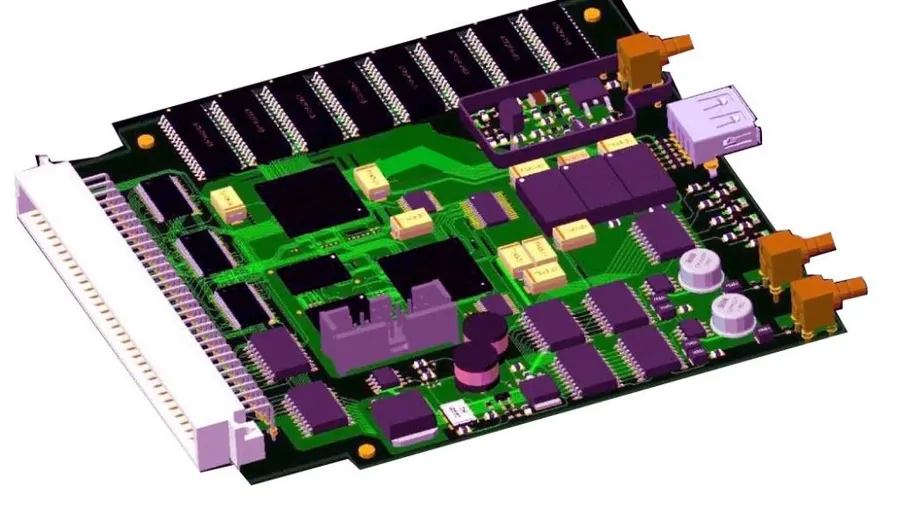
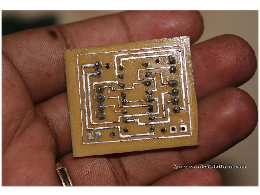
A Printed Circuit Board (PCB) serves as the foundational platform for electronic circuits, providing both mechanical support and electrical connections for components. The 'why DIY' aspect stems from the desire for customization, rapid prototyping, and educational exploration, enabling individuals to translate unique electronic ideas into physical realities.
PCBs are composed of a non-conductive substrate, typically fiberglass or composite materials, onto which conductive copper traces are patterned. These traces act as electrical pathways, connecting various components such as resistors, capacitors, and integrated circuits. The structure is often multi-layered, consisting of alternating layers of conductive and insulating material, increasing the board's functionality and reducing space.
Advantages of DIY PCB Making Creating PCBs at home offers significant advantages, primarily in terms of customization and cost control. It allows for rapid iteration of designs, making it ideal for prototyping and experimentation. This flexibility is especially beneficial for hobbyists, students, and small-scale projects.
Educational Value The DIY approach to PCB making also has immense educational value. It facilitates a deeper understanding of electronics design, manufacturing processes, and troubleshooting, providing hands-on experience that cannot be replicated through theoretical learning alone. It bridges the gap between abstract concepts and real-world application.
Cost Efficiency Although initial investment in materials and equipment is required, in the long term, DIY PCB fabrication can be more cost-effective than using professional services for prototyping or small production runs. DIY allows for control over material choices and design complexities, which can lead to cost savings, particularly for repeated or iterative designs.
Aspect
DIY PCB
Professional PCB
Customization
High, tailored to specific needs
Limited to predefined options
Cost
Lower for small quantities and prototypes
Higher for small quantities but lower for large batches
Lead Time
Fast, immediate iteration
Longer, depends on production schedule
Control
Full control over design and materials
Less control, standard processes
Quality
Variable, depends on skills and equipment
High, standardized manufacturing
Learning
Extensive hands-on learning
Limited direct learning
Essential Materials and Tools for Your DIY PCB Maker Setup
PCB Fabrication Tools
Creating your own printed circuit boards (PCBs) at home requires a specific set of materials and tools. This section provides a comprehensive overview of what you'll need to get started, ensuring a smooth and efficient DIY PCB fabrication process.
Material/Tool
Description
Purpose
Considerations
Copper Clad Boards
Sheets of non-conductive material (typically fiberglass or FR4) with a thin layer of copper on one or both sides.
Base material for creating circuit traces.
Select single or double-sided based on complexity of your circuit; FR4 is most common, various sizes and thicknesses are available.
Laser Printer
High-resolution printer using toner, not inkjet.
Essential for transferring the circuit design onto the transfer paper.
Ensure printer's toner adheres well to transfer paper, and can handle various paper weights; may be repurposed.
Transfer Paper/Film
Specialized paper or film designed for toner transfer to copper.
Used to transfer printed circuit design onto the copper clad board.
Different types have varying release qualities and toner adhesion; choose quality material for best results.
Etchant
Chemical substance used to remove unwanted copper.
Removes copper that is not part of the desired circuit.
Ferric chloride is common, but hydrochloric acid/hydrogen peroxide is a faster, more potent alternative; must be handled carefully.
Etching Container
Acid resistant container to hold etchant and PCB
Holds the etching solution and PCB during etching.
Choose a plastic or glass container that is chemically resistant and large enough to fully submerge your board.
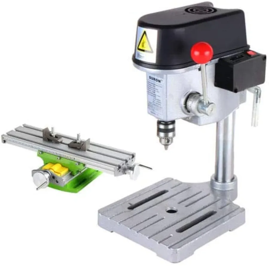
Drilling Machine (Hand Drill/Drill Press)
Used to create through-holes for component leads.
Drill accurate holes in the PCB board for component placement.
A drill press offers better accuracy and stability. Consider a variable speed drill.
Drill Bits
Specialized small drill bits for PCB drilling.
Used for creating the holes for through-hole components.
Use small drill bit sizes such as 0.8, 1.0 and 1.2mm, as needed. Purchase quality carbide drill bits for best longevity.
Safety Glasses
Protective eyewear.
Protects eyes from chemical splashes or flying debris.
Essential for all stages of PCB making, prioritize safety. Always wear when working with chemicals or drilling.
Gloves
Chemical-resistant gloves.
Protects skin from etchants and other chemicals.
Ensure gloves are rated for the chemicals you are using. Nitrile gloves are common.
Tweezers or Forceps
Small tools for handling small components and delicate materials.
Used for handling small components or delicate materials, applying solder mask, etc.
Choose tweezers with fine tips for precision work. Consider stainless steel.
Ruler or Calipers
Precision measuring tools.
Used for accurate measurement of board dimensions and hole placement.
Digital calipers offer high precision measurements.
Cleaning Supplies
Acetone, isopropyl alcohol, soft cloths or paper towels
Used for cleaning the board of residue, toner or ink after etching and before assembly.
Use residue free cleaners like pure acetone or isopropyl alcohol.
Permanent Markers
Used for touchups on the toner transfer for better etching result
Touch up any gaps or errors in the toner transfer.
Ensure it's resistant to the etching solution.
Designing Your PCB Layout: Software and Techniques for DIY PCB Makers
PCB Design Software
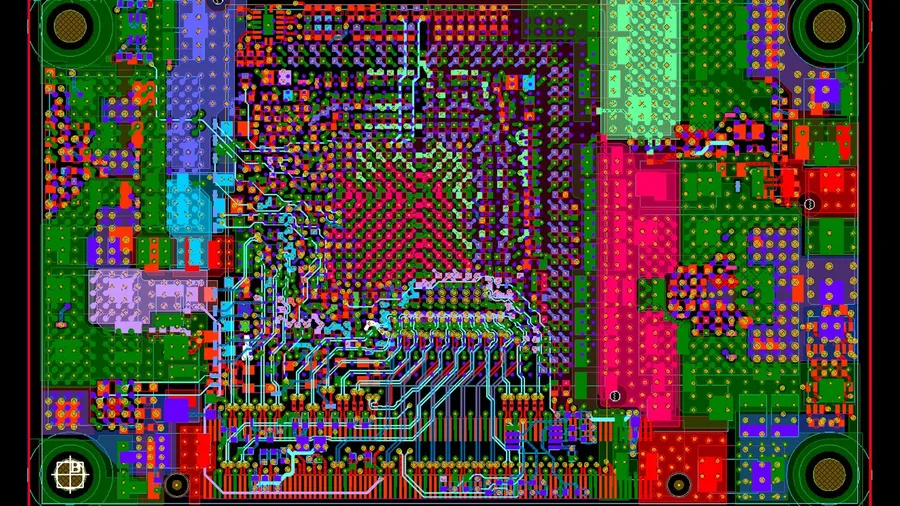
Creating a precise PCB layout is a crucial step for any DIY PCB maker. This involves using specialized software to design the circuit's physical arrangement, ensuring proper connections and spacing for components before physical fabrication. This section provides a practical guide to using PCB design software for optimal results.
Key considerations during the PCB design process:
Schematic Capture Begin by creating a schematic diagram representing the electrical connections of your circuit.
Component Footprints Select appropriate footprints for your components, ensuring they match your physical parts for correct placement.
Board Outline Define the physical dimensions of your board, taking into account any space constraints for your project.
Component Placement Strategically place components on the PCB, prioritizing signal flow and ease of soldering.
Routing Draw the traces (conductive paths) connecting the components, adhering to design rules to avoid short circuits or signal interference.
Design Rule Check Use the software's design rule checker to identify any errors in your layout, such as insufficient spacing or routing conflicts.
Free PCB Design Software Options:
Software
Description
Key Features
KiCad
Open-source suite for schematic capture and PCB layout
Cross-platform, extensive component library, active community support
EasyEDA
Web-based PCB design tool
User-friendly interface, integrated component library, collaboration features
DesignSpark PCB
Free software from RS Components
Easy to use interface, built-in component library and BOM (Bill of Materials) management.
Using KiCad: A Step-by-Step Guide
Install KiCad Download and install the latest version of KiCad from the official website.
Create a New Project Launch KiCad and create a new project directory. Start by designing the schematic diagram of your circuit.
Add Components Add the required components to your schematic diagram by selecting them from KiCad's library.
Wire Components Connect the components using KiCad's 'wire' tool, forming your electronic circuit.
Switch to PCB Layout Generate a netlist of your schematic and switch to the PCB layout editor.
Place Footprints Position the footprints of the components, based on the physical dimensions you plan for your board.
Route Traces Draw the traces to connect the components according to your schematic. Utilize KiCad's routing tools, keeping width considerations in mind, especially if current will be passing through the traces.
Design Rule Check Run the design rule checker (DRC) to detect any errors. Resolve any conflicts or errors as detected by DRC
Export Gerber Files Export the gerber files of the design, ready to be printed/transferred to the physical copper clad board.
Transferring the PCB Design: Methods and Best Practices
Toner Transfer PCB
Accurately transferring your PCB design onto the copper clad board is a pivotal step in the DIY PCB fabrication process. This stage requires precision to ensure the final etched circuit matches your design. Several methods are available, each with its advantages and best practices, with the most common being the toner transfer method.
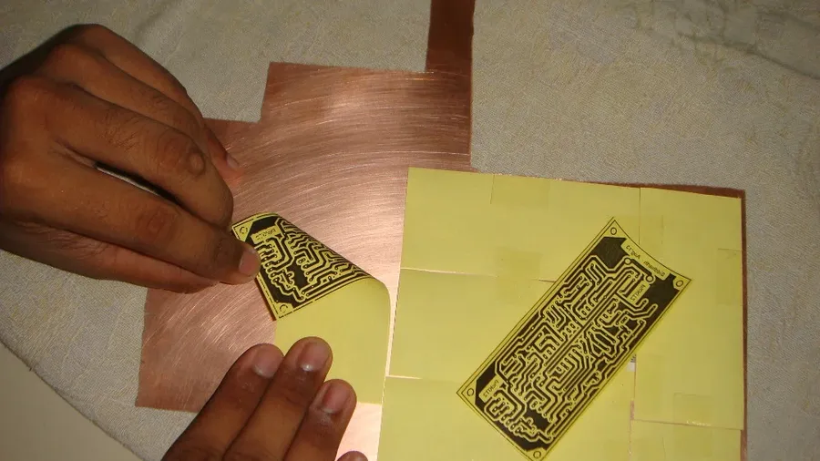
The toner transfer method utilizes the heat and pressure of a standard laser printer and laminator or clothes iron to adhere toner from a printed design onto the copper board. When done correctly, the toner acts as an etch-resistant barrier, defining the conductive traces on your PCB.
Toner Transfer Method Using Laser Printer This method involves printing your PCB layout onto specialized transfer paper using a laser printer. The toner acts as an etch resist when transferred onto the copper clad board. Carefully aligning the printed design with the copper board is critical to ensure the final etched circuit aligns with the design.
Using Specialized Transfer Paper or Film Specialized transfer paper or film is designed to release the toner when heated, this facilitates a clean transfer onto the copper board. The use of correct settings on the printer can ensure that sufficient toner is applied for the transfer process. After the transfer, gently peel the paper off, leaving the toner on the copper surface.
Ensuring Accurate Alignment Accurate alignment is vital, ensure the printed PCB layout matches your board dimensions and is placed without skew or offset. Using alignment marks on the PCB design and matching these to edges of the PCB can assist in achieving good alignment. Secure the paper to the board to avoid slippage during the transfer process.
Heat and Pressure Application Consistent heat and pressure are essential for a successful toner transfer. Use a laminator or clothes iron to apply heat to the transfer paper. Applying even pressure across the entire design area and maintain correct heat settings to allow the toner to adhere effectively to the copper board, avoid moving the paper during the process. Uneven heat or pressure can result in an incomplete or distorted transfer.
Method
Description
Advantages
Disadvantages
Toner Transfer with Laser Printer
Uses laser printer and heat to transfer toner to PCB
Can require multiple attempts, transfer quality may vary
Direct Printing Methods
Uses special printer to directly print on the PCB
Very high precision
Higher initial investment in equipment
Photolithography
Uses UV light to transfer design onto photoresist coated PCB
Very precise, well suited to fine details
More complex process, requires more materials and equipment
Etching Your PCB: Chemical and Safe Handling Guidelines for DIY PCB Makers
PCB Etching
The etching process is crucial in DIY PCB fabrication, where unwanted copper is removed from the board, leaving behind the desired circuit traces. This process typically involves chemical etchants, and requires careful execution with safety considerations as a priority. It is essential for achieving the desired conductivity and functionality of the printed circuit board.
Key considerations for successful etching include selecting the appropriate etchant, accurately timing the etching process to avoid over or under-etching, and safely handling and disposing of chemical etchants. Safety gear such as gloves, goggles, and proper ventilation are indispensable when performing etching.
Etchant
Chemical Formula
Concentration
Etching Time
Safety Notes
Disposal Method
Ferric Chloride
FeCl3
30-40% solution
20-40 minutes
Wear gloves and goggles, avoid inhalation
Neutralize with sodium carbonate, dispose as hazardous waste
Hydrochloric Acid & Hydrogen Peroxide
HCl & H2O2
1:2 HCl:H2O2 (30% H2O2)
5-15 minutes
Wear gloves, goggles, and respirator, work in well-ventilated area
Dilute with water, neutralize, dispose of as hazardous waste
Preparation Ensure your PCB layout is completely transferred to the copper clad board, either by the toner transfer method or photoresist, before starting the etching process. Check that your resist is not peeling or has any defects.
Etching Process Submerge the board into the selected etchant. Gently agitate the solution or the board to ensure uniform etching. Monitor the process closely to prevent over-etching, which is where copper is removed beyond the intended traces and pads.
Rinsing Once etching is complete, quickly rinse the board with clean water. This halts the etching process and removes the etchant residue from the board surface.
Resist Removal Use a suitable solvent to remove the resist (toner or photoresist). Isopropyl alcohol (IPA) is often used to remove toner and a specific resist remover, if using photoresist. This reveals the copper traces. Thoroughly clean the PCB and dry it.
Inspection Visually inspect the PCB for any errors or imperfections. Pay close attention to the etched traces, checking for any breaks, shorts, or over-etching. Ensure that all pads are properly formed and ready for component placement.
Safety Precautions Always wear appropriate safety equipment, including gloves, goggles, and a lab coat, and work in a well-ventilated area to prevent exposure to harmful chemicals. Follow the MSDS safety data sheets for the chemicals.
Disposal Properly dispose of used etchant and waste as hazardous waste. Never pour chemicals down the drain, or into the environment. Neutralize the etchant when required and dispose of the etchant according to local regulations.
Drilling and Finishing Your DIY PCB: Preparing for Assembly
PCB Drilling
After etching, the DIY PCB requires drilling and finishing to prepare it for component assembly. This involves creating precise holes for component leads, cleaning the board to remove residue, and applying a solder mask to protect traces and facilitate soldering. These steps are crucial for a functional and reliable final product.
The drilling process is a critical stage that requires precision and appropriate tools to ensure accurate placement of components. Following drilling, finishing tasks like cleaning and solder mask application play a pivotal role in protecting the board, and improving solderability.
Drilling Holes Use a drill press or a hand drill with a precision drill bit set, selecting the correct size for different component lead diameters. Start with small pilot holes and gradually increase to the required size. Always drill straight and avoid applying excessive pressure which can damage the PCB.
Deburring After drilling, gently remove any burrs or rough edges around the holes using a deburring tool or fine sandpaper. This prevents shorts and ensures components sit flush against the board.
Cleaning the PCB Clean the PCB thoroughly with a suitable solvent, such as isopropyl alcohol, to remove any remaining etchant, dust, or other debris. Ensure the board is completely dry before proceeding to the next step.
Applying Solder Mask Apply a solder mask, which can be a commercially available spray, or a DIY solder mask solution applied with a brush. This helps to protect the copper traces from oxidation, preventing accidental solder bridges during assembly, and providing a more professional finish.
Curing the Solder Mask Allow the solder mask to cure completely according to manufacturer instructions or curing under UV light, making sure the solder mask is dry before any further operations.
Final Inspection Inspect the PCB to ensure the drilled holes are accurate, the board is clean, and the solder mask is applied correctly. Address any issues before assembly.
Step
Tools
Material
Purpose
Drilling Holes
Drill press or hand drill with precision drill bit set
Appropriate size drill bits
Create holes for component leads
Deburring
Deburring tool or fine sandpaper
N/A
Remove burrs and rough edges
Cleaning the PCB
Soft cloth or brush
Isopropyl alcohol or other suitable solvent
Remove residues and contaminants
Applying Solder Mask
Spray can or brush
Solder mask liquid
Protect traces and enhance solderability
Curing the Solder Mask
UV lamp or curing oven (depending on type)
N/A
Harden solder mask
Frequently Asked Questions About DIY PCB Making
This section addresses common questions that arise when individuals delve into the world of DIY PCB fabrication. It covers the practical aspects, cost considerations, and design challenges frequently encountered by those making circuit boards at home.
Can I make my own PCB at home? Yes, it is absolutely feasible to create your own PCBs at home using a variety of methods. The most common techniques include toner transfer, chemical etching, and, for more advanced applications, CNC milling or UV exposure of photosensitive film. These methods allow hobbyists and enthusiasts to produce circuit boards for personal projects.
What is the most cost-effective way to make a PCB? The toner transfer method coupled with chemical etching is generally the most cost-effective way for DIY PCB creation. This method primarily uses a laser printer, specialized transfer paper or film, a common etchant like ferric chloride, and readily available materials. While it may not achieve the precision of more expensive methods, it's perfect for prototyping and single-layer PCBs.
What is the simplest method to create a PCB by hand? The most basic method to create a PCB by hand involves drawing the circuit layout directly onto a copper clad board using an etch-resistant marker or pen and then etching the board. Although not precise, it's suitable for the simplest circuits, and for learning the basic principles of PCB fabrication. This method avoids the use of printers or sophisticated transfer techniques.
How challenging is it to design my own PCB layout? The difficulty of designing a PCB layout depends largely on the complexity of the circuit. With the help of user-friendly, free software packages like KiCad or Eagle, beginners can create basic layouts relatively easily. However, complex designs with densely packed components and multi-layer routing demand a higher degree of skill and experience. Learning curve is also influenced by the individual's prior experience with electronic schematics.
What safety precautions should I take when etching PCBs? Safety is paramount when etching PCBs, primarily due to the use of corrosive chemicals. Always wear appropriate personal protective equipment (PPE) like gloves, safety goggles, and a lab coat. Work in a well-ventilated area to avoid inhaling fumes. When disposing of etchants, neutralize them before discarding in accordance with local environmental regulations. Proper storage of these chemicals is also crucial to prevent accidental spills or reactions.
Can I make double-sided PCBs using DIY methods? Yes, double-sided PCBs can be made at home using DIY methods, although they do require more precision and care. The key challenge is aligning the patterns for both sides of the board accurately. Techniques include using alignment pins or very precise double-sided transfer methods to minimize misalignments and to avoid shorts.
What are common pitfalls to avoid when making PCBs at home? Common pitfalls include inadequate toner transfer leading to missing tracks, over-etching causing thin or broken traces, and poor drilling resulting in misaligned components. Ensuring proper preparation, thorough cleaning of the copper clad board, accurate application of the toner transfer, precise etching duration, and proper drilling practices can prevent most issues. Careful planning and attention to detail are key to success.
Troubleshooting Common Issues in DIY PCB Making
Even with careful planning, DIY PCB fabrication can present challenges. This section provides actionable solutions to common problems, ensuring a smoother PCB making process by addressing issues such as poor transfer quality, over-etching, and broken traces.
Poor Toner Transfer Quality Inadequate toner transfer often results in incomplete or distorted patterns on the copper board, causing issues during etching. To resolve this, ensure your laser printer is set to the highest toner density and the paper/film is properly applied to the copper board, using even and sufficient heat during transfer. Also, consider the type of paper or film; specialized transfer media can significantly improve results. Clean the copper surface meticulously prior to transfer to ensure proper adhesion of the toner.
Over-Etching Over-etching occurs when the etchant removes too much copper, leading to thin traces or loss of pads. This is often due to excessive etching time or an overly concentrated etchant solution. To prevent over-etching, carefully monitor the etching process. Regularly check the board and remove it from the etchant as soon as the unwanted copper is dissolved. Dilute the etchant solution if necessary, and maintain an optimal temperature as excessive heat will speed up the reaction. Consider agitating the solution during etching for even material removal.
Broken Traces Broken traces can result from several causes, including poor initial transfer, aggressive etching, or physical damage after etching. Inspect the transfer carefully for any breaks before etching, and use a fine-tipped pen to repair any minor breaks in the toner pattern before etching. Handle the PCB gently during and after etching. If breaks appear post-etching, they can be repaired with fine wire or conductive pen. Prevention through good transfer practices is key to minimizing broken traces.
Residue After Etching Residue left after etching can interfere with soldering and component placement. Thoroughly cleaning the PCB with appropriate solvents such as acetone or isopropyl alcohol immediately after etching is crucial. Use a soft brush to remove any stubborn residues. Post-cleaning inspection under magnification can help identify and address any missed areas.
Incomplete Etching Incomplete etching happens when the etchant hasn't removed all of the exposed copper, leaving behind unwanted conductive material. This is usually due to insufficient etchant concentration, inadequate temperature, or insufficient time in the etchant solution. To solve this, ensure the etchant is freshly prepared or not depleted. Maintain the etchant at the optimal temperature and stir the solution periodically to aid the process. If these don’t address the problem, carefully place the PCB back into the etchant for a bit longer, monitoring closely for completion.
Exploring Alternative DIY PCB Techniques and Advanced Methods
CNC PCB Milling
While the previously discussed methods form the foundation of DIY PCB creation, several advanced techniques offer increased precision and capabilities for the ambitious maker. These methods, such as CNC milling and photosensitive film processes, cater to more complex circuit designs and higher production quality demands.
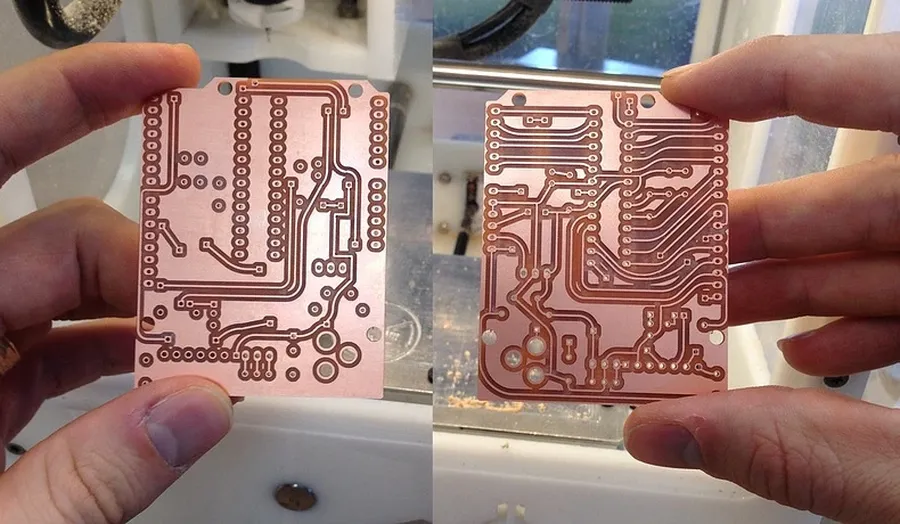
CNC Milling Computer Numerical Control (CNC) milling utilizes a precision machine to carve away copper from a PCB blank based on a digital design. This method offers a high degree of accuracy and repeatability, and is suitable for double-sided boards and fine-pitch components. It eliminates the need for chemicals, making it a cleaner alternative to etching, although it requires a higher initial investment in equipment.
Photosensitive Film Method This technique employs a photosensitive dry film laminate applied to the copper clad board. After exposing the film to UV light through a transparent mask with the PCB design, the exposed film hardens, and the unexposed film is washed away. The copper is then etched using standard etchants. The photosensitive film method allows for more intricate designs than toner transfer.
Direct Laser Engraving Direct laser engraving is a cutting-edge technique where a laser is used to remove the protective coating from the copper clad board directly, eliminating the need for a physical mask. After the protective coating is removed, the etching process is similar to the standard procedure. This method offers the advantage of high precision and speed, reducing the time required to create a PCB board. This method usually requires more expensive equipment.
Technique
Accuracy
Equipment Cost
Process Complexity
Chemical Use
CNC Milling
High
High
Medium
None
Photosensitive Film
High
Medium
Medium
Yes
Direct Laser Engraving
Very High
High
Medium
Yes
Creating your own PCBs is a journey from concept to reality. As a DIY PCB maker, you've learned to harness the tools and techniques necessary to bring your electronic ideas to life. Whether you're prototyping a new invention, exploring the world of electronics, or simply enjoying the challenge, the skills you have gained are a testament to your innovation and persistence, paving the way for future creative projects.