In today's fast-paced electronics industry, rapid prototyping is crucial. The BotFactory SV2 PCB printer emerges as a game-changer, enabling engineers to create functional PCBs right on their desktop. This article delves into the features and advantages of the SV2, showcasing how it streamlines the design and manufacturing process, like transforming a sketch into a real circuit board within hours, and is at the forefront of the industry.
Understanding the BotFactory SV2 PCB Printer
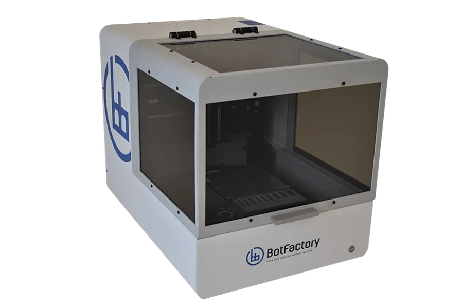
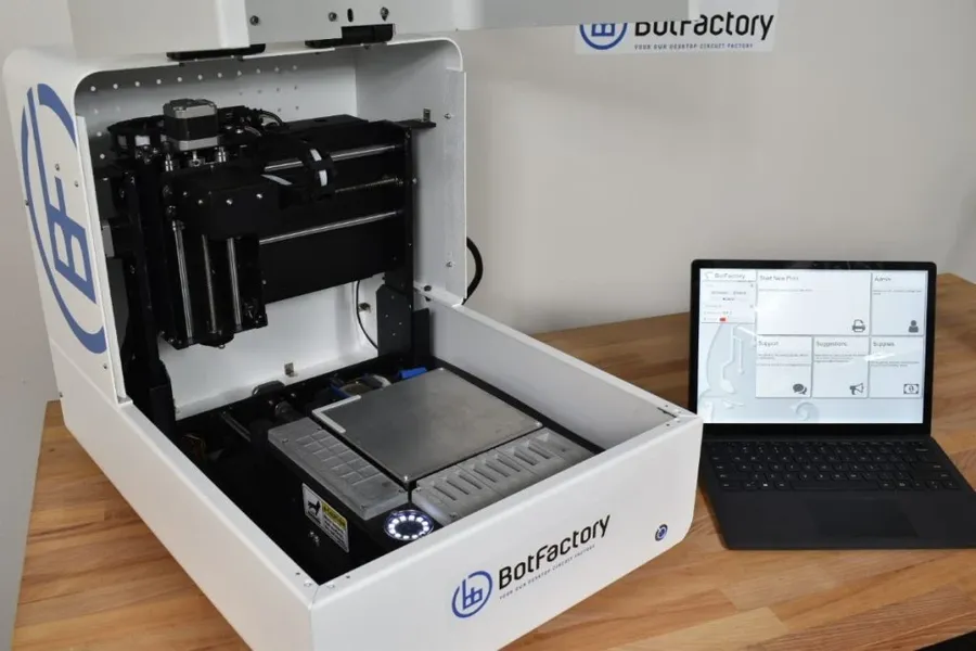
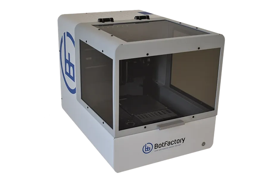
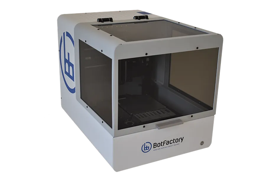
BotFactory SV2 PCB printer
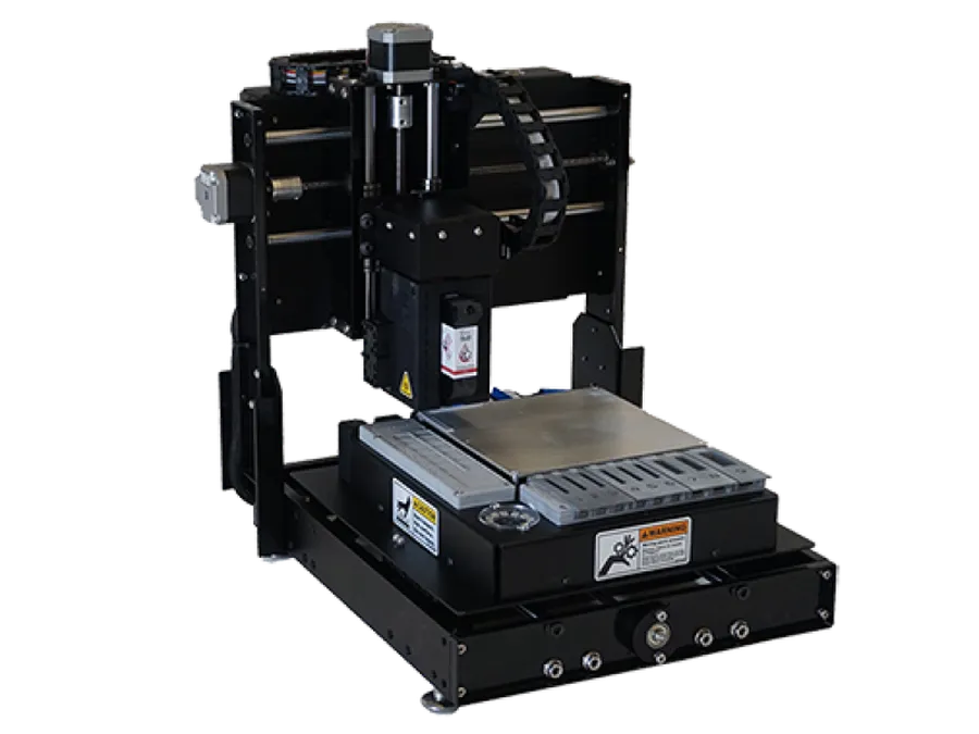
The BotFactory SV2 is a revolutionary all-in-one desktop PCB printer designed to streamline the prototyping process, departing significantly from traditional PCB manufacturing methods. It integrates multiple functionalities, including material deposition, pick-and-place component placement, and multi-layer printing into a single machine, enabling rapid fabrication of functional circuit boards directly from digital designs.
Unlike conventional methods that often involve outsourcing, which introduces delays and costs, the BotFactory SV2 allows engineers and researchers to prototype boards in-house, reducing lead times and enabling quick design iterations. Its ability to handle a variety of materials and perform component assembly further enhances its versatility and simplifies the workflow from design to a fully assembled PCB.
Key Features of the BotFactory SV2
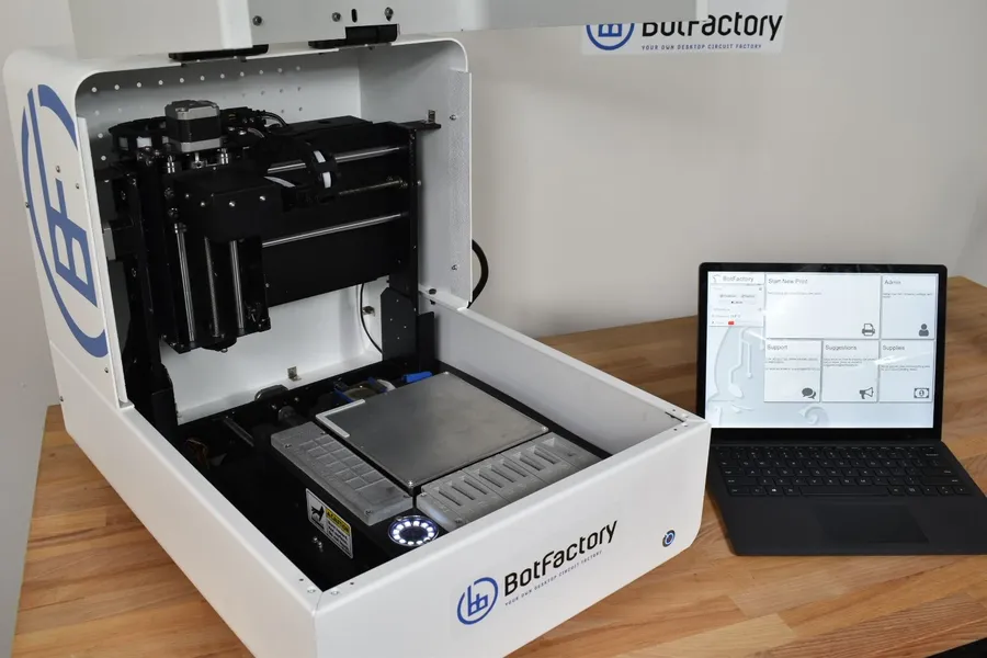
BotFactory SV2 features details
The BotFactory SV2 stands out as a comprehensive solution for in-house PCB prototyping, characterized by its multi-faceted capabilities that streamline the fabrication process from design to functional board. Its core strengths lie in its multi-material printing, automated pick-and-place functionality, and high precision in creating multi-layer PCBs, enabling rapid and efficient prototyping of complex electronics.
Multi-Material Printing The SV2 supports a variety of functional inks, including conductive, resistive, and dielectric materials, allowing for the direct printing of traces, components, and insulation layers on a single platform. This eliminates the need for multiple machines and processes.
Automated Pick-and-Place Integrated component placement significantly enhances the printer's capabilities. With automated pick-and-place functionality, the SV2 can accurately place surface-mount components onto the printed substrate, which further minimizes manual assembly and potential human errors.
High-Precision Multi-Layer PCB Creation The BotFactory SV2 can fabricate multi-layer boards with high precision and accuracy. The ability to print and stack layers directly ensures correct alignment and interconnectivity, which is crucial for complex circuit designs. This capability enables the creation of prototypes that closely mirror the final product.
Rapid Prototyping Capabilities With its integrated printing and assembly functions, the SV2 dramatically reduces turnaround time from design to prototype. The ability to produce complex PCBs in-house enables rapid design iterations, facilitating quicker time-to-market for new products or research findings.
Feature
Description
Multi-Material Printing
Enables the printing of conductive traces, insulators, and resistors directly onto the substrate.
Automated Pick-and-Place
Facilitates precise placement of surface-mount components.
Multi-Layer Capability
Allows the creation of PCBs with multiple interconnected layers.
Rapid Turnaround
Offers quick prototyping times with in-house fabrication.
Precision
High accuracy in printing and component placement crucial for complex boards.
BotFactory SV2 Models: Pro, Enhanced, and Premium
BotFactory SV2 Pro
The BotFactory SV2 is available in multiple models, each tailored to different user needs and production demands. The Pro, Enhanced, and Premium models offer varying capabilities, primarily differing in their layer printing capacity and advanced features, allowing users to choose the best variant for their specific PCB prototyping requirements.
Feature
SV2 Pro
SV2 Enhanced
SV2 Premium
Maximum Layer Count
6
4
8+
Precision
High
High
Ultra-High
Automated Pick-and-Place
Standard
Standard
Advanced
Multi-Material Printing
Yes
Yes
Yes
Advanced Inks Support
Yes
Limited
Extensive
Best Suited For
Complex Multi-Layer PCBs
Standard Multi-Layer PCBs
High-Precision R&D and Production
The SV2 Pro is designed for users needing complex, multi-layer PCBs, offering a maximum of 6 layers. The SV2 Enhanced is a cost effective solution that is suitable for users that need standard multi-layer PCBs, supporting up to 4 layers. The SV2 Premium is designed for users that need maximum precision and advanced features, offering 8+ layers, advanced automated pick and place and extensive ink support.
The SV2's Process: From Gerber Files to Functional Boards
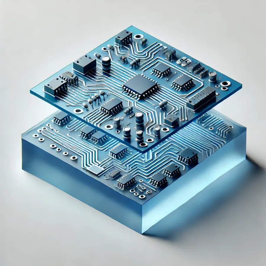
SV2 printing PCB process
The BotFactory SV2 streamlines PCB fabrication by integrating design, material deposition, and component placement into a single, automated workflow. This section provides a step-by-step guide on using the SV2, from Gerber file generation to the creation of functional circuit boards.
Exporting Gerber Files from KiCAD EDA Begin by finalizing your PCB layout in KiCAD. Export Gerber files for each layer (copper, silkscreen, solder mask, etc.) and the drill file. Ensure all dimensions and parameters align with the SV2's specifications.
Preparing the SV2 Software Import the exported Gerber files into the SV2's software. This software will allow you to set parameters like printing layers, material selection for each layer, trace width, spacing, and any other important printing parameters. Ensure all materials are calibrated correctly.
Material Loading and Calibration Load the selected conductive and insulating inks, as well as other necessary materials, into the SV2's dispensing system. Perform a material calibration procedure to ensure proper ink flow and layer height for accurate printing. This ensures consistent and precise deposition during the fabrication process.
Printing Conductive Layers Initiate the printing process. The SV2 will selectively deposit conductive ink onto the substrate, forming the circuit traces and pads according to the imported Gerber data. Observe the process and make adjustments if necessary.
Printing Insulating Layers If your design includes multi-layer PCBs, load the insulating ink and use the SV2 software to print the required insulating layers according to the Gerber data. These layers form the substrate for subsequent conductive layers and prevent short circuits.
Solder Paste Deposition (Optional) If the design includes components, use the SV2 to selectively deposit solder paste onto the component pads. The SV2's pick-and-place feature is available to accurately place surface mount components, after solder paste deposition.
Component Placement and Curing Using the integrated pick-and-place system, populate the board with surface mount components as specified in the design. Once all components are placed, a curing process (usually involving heat or UV light) is required for the inks and solder paste.
Functional Testing and Validation After the curing phase, the printed board is ready for testing. Verify the functionality using standard electronic testing procedures.
Materials and Compatibility with SV2
Materials used for BotFactory SV2
The BotFactory SV2's versatility is significantly enhanced by its compatibility with a range of specialized materials, primarily conductive and insulating inks. These materials are crucial for creating functional PCBs directly from digital designs, providing a streamlined prototyping process. Understanding the properties and limitations of these materials is essential for successful PCB fabrication with the SV2.
Enables direct printing of circuit traces; good electrical conductivity; suitable for rapid prototyping.
Can have lower conductivity than traditional copper; may require multiple passes to achieve desired trace thickness; prone to oxidation; not suitable for high-frequency application.
Circuit Traces, Via connections, Basic interconnects
Insulating Inks
Non-conductive inks used to create insulating layers and define the layout of the board.
Provides electrical isolation; essential for creating multilayer PCBs; compatible with conductive inks.
Limited mechanical strength; not suitable for structural applications; some may require UV curing.
Used to form mechanical and electrical connections by melting to join components on a PCB
Allows for reflow soldering with components directly on the printed PCB; provides strong bond and good conductivity.
Requires reflow oven; may need stencils to control the application precisely.
Surface mount component attachment.
Adhesives
Used to attach components to PCBs
Allows for strong and permanent bond of components to a PCB, good mechanical strength.
Adhesive may require special heating or curing conditions.
Component attachment.
The BotFactory SV2 also accommodates specific substrates, typically flexible polymer films or rigid FR4 sheets, chosen for their compatibility with the inks and their mechanical properties for the board being printed. It's important to ensure the materials are compatible with the printer settings and required application.
Benefits of In-House PCB Manufacturing with the SV2
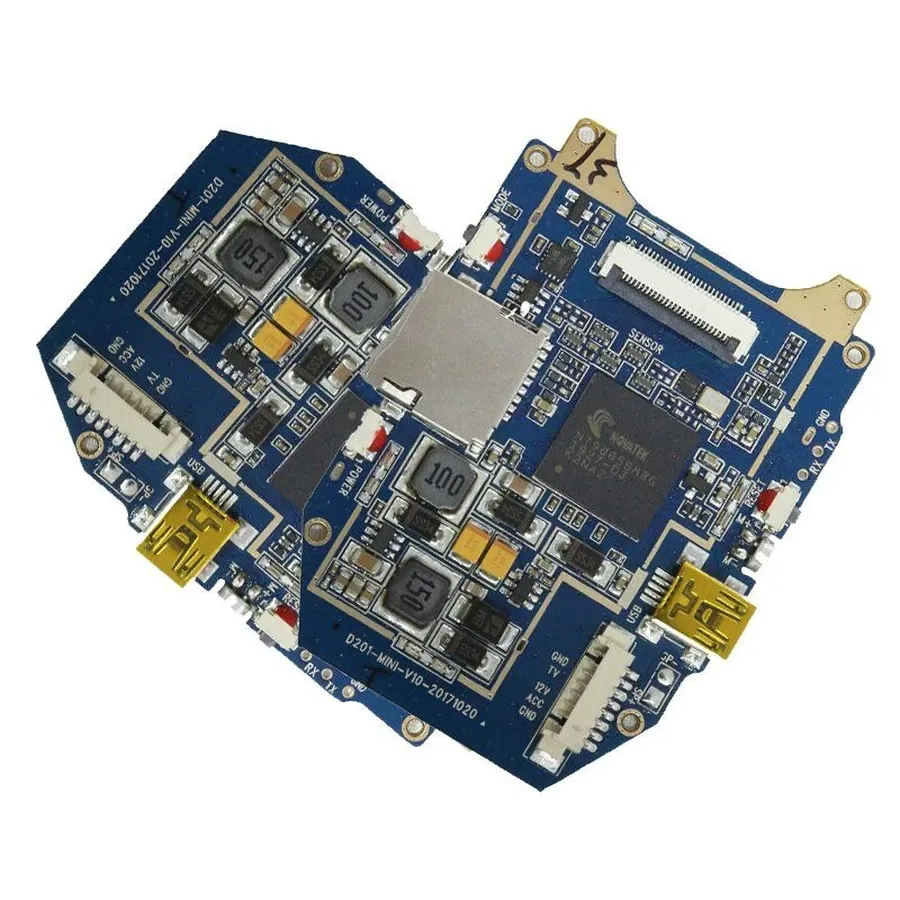
PCB board produced by SV2
The BotFactory SV2 significantly streamlines PCB prototyping by enabling in-house fabrication, offering distinct advantages over traditional outsourcing models. This approach addresses key pain points associated with conventional manufacturing, such as extended lead times, high costs, and limited control over the production process.
Accelerated Design Cycles In-house prototyping with the SV2 drastically reduces turnaround times. Designers can iterate rapidly and test new designs within hours, not weeks, accelerating the overall development cycle. This eliminates the delays associated with waiting for external manufacturers.
Reduced Costs While there is an initial investment in the SV2, it leads to long-term cost savings by eliminating the per-unit costs associated with traditional PCB fabrication. This is particularly beneficial for projects with multiple design revisions or low-volume production needs.
Enhanced Control over Prototyping The SV2 provides complete control over the entire fabrication process, allowing engineers to tweak parameters and experiment with materials on-demand. This direct control minimizes the risks of miscommunication and design misinterpretations that often arise with outsourcing.
Minimized Manufacturing Bottlenecks By eliminating reliance on external manufacturers, research teams can significantly reduce production bottlenecks. The ability to prototype in-house allows for continuous experimentation and immediate design validation, fostering faster innovation.
Greater Design Flexibility With the SV2, creating complex PCB designs becomes more feasible. The in-house control allows for rapid experimentation with various layout configurations and intricate features. This flexibility is especially advantageous for advanced R&D activities.
IP Protection and Security Keeping PCB prototyping in-house protects sensitive design information. By avoiding outsourcing, companies can ensure better control over their intellectual property, safeguarding against potential breaches or unauthorized access.
Frequently Asked Questions About the BotFactory SV2 PCB Printer
This section addresses common inquiries regarding the BotFactory SV2, providing practical answers about its cost, setup process, operational maintenance and more, drawing from frequent user searches.
What is the typical price range for the BotFactory SV2 PCB printer? The BotFactory SV2 is a professional-grade prototyping system, and its price reflects its capabilities. It's best to directly contact BotFactory or authorized resellers for the most accurate and up-to-date pricing. The cost can vary based on the specific model (Pro, Enhanced, or Premium) and any additional accessories or support packages you may require. Consider the long-term savings in time, resources, and outsourcing costs when assessing the initial investment.
Where can I find the BotFactory SV2 PCB printer manual? The official BotFactory SV2 user manual is usually provided with the purchase of the printer. It can also be downloaded from the BotFactory website, under their support documentation section. Be sure to download the manual specific to your SV2 model. The manual will be vital in the initial setup, operation and maintenance of the equipment.
What is involved in the setup of the BotFactory SV2 PCB printer? Setting up the BotFactory SV2 involves unpacking the printer, connecting it to the required power and network connections and installing the required software. Detailed setup steps are given in the user manual. The SV2 also requires calibration of its print head before use. It is recommended to allocate some time to review the manual and practice on some test prints before attempting to make full functional circuits.
What kind of maintenance is required for the BotFactory SV2? The BotFactory SV2 requires regular maintenance to ensure it runs smoothly. This includes cleaning the printer head, replacing the ink cartridges, and verifying calibration as necessary. Regular cleaning is essential to avoid clogs and buildup of material that may affect the quality of the printed PCB. The detailed maintenance process is outlined in the user manual, and preventative maintenance is the best approach to prolonging the useful life of the printer.
How complex of a PCB can the BotFactory SV2 print? The BotFactory SV2 is capable of printing complex multi-layer PCBs, depending on the model type. The Pro model can handle up to 6 layers, while other models like the Enhanced model can handle up to 4 layers. The specific limitations will be defined in the product specification for each model. The complexity is not only limited to the number of layers but also the complexity of the design, which must meet the resolution capabilities of the SV2.
What types of materials can the BotFactory SV2 utilize? The BotFactory SV2 supports a variety of specialized conductive and dielectric inks, allowing for the creation of fully functional PCBs. The range of materials will include inks that are used for the conductive traces and other inks that will be used for the insulating layers. The product specifications will list all materials compatible with each printer model, and care must be taken to ensure that only recommended materials are used to avoid damage to the unit.
Is the BotFactory SV2 suitable for high-volume production? The BotFactory SV2 is primarily designed for rapid prototyping and low-volume production runs. It's ideal for research, educational settings, and companies that require flexibility and quick turnaround in their design process. The SV2 is not the best choice for large scale production as traditional manufacturing offers better scalability and cost efficiency for large batch runs. If your needs are for prototyping and low volume this machine will do the job well.
SV2 vs Traditional PCB Manufacturing
Small Batch Prototypes
The BotFactory SV2 represents a paradigm shift in PCB fabrication, moving away from traditional manufacturing processes. This section provides a feature-by-feature comparison, emphasizing key differences in speed, cost, and design flexibility between the SV2 and conventional PCB manufacturing methods.
Feature
BotFactory SV2
Traditional PCB Manufacturing
Turnaround Time
Hours (for simple designs), days(for complex design) immediate for basic layer and component placement.
Days to weeks, depending on complexity and vendor lead times.
Cost
Moderate initial investment, lower per-board cost for prototyping and small runs.
Lower per-board cost for large production runs, significant upfront costs for small or custom runs.
Design Flexibility
Highly flexible, allows rapid iterations and modifications directly in-house.
Limited flexibility, design changes are expensive and time-consuming.
Layer Count
Up to 6 layers (Pro model), up to 4 layers (Enhanced)
Typically 2-32+ layers depending on the process, but at a higher cost
Setup
Relatively quick and straightforward setup process, requiring minimal operator training.
Complex setup processes involving multiple vendors and longer lead times.
Material
Compatible with a range of conductive and insulative inks and solder paste, requires specific ink types
Variety of standard materials such as FR-4, metal layers (copper), etc.
Tooling & Setup
Minimal setup and tooling. Software based design with in-house printing and assembly
Requires external fabricator, setup and design rules. Requires significant expertise.
Prototyping
Highly suitable for rapid prototyping and design iterations.
Slow and expensive for prototyping
Use Cases: Where the SV2 Shines
Application of PCB board printed by SV2
The BotFactory SV2 excels in environments requiring rapid prototyping, agile design iterations, and on-demand PCB fabrication. Its versatility makes it valuable across diverse sectors, including research, education, and specialized manufacturing. The SV2's unique capabilities are best illustrated through its application in practical, real-world scenarios.
Rapid Prototyping In fast-paced product development cycles, the SV2 significantly shortens the time between design and functional prototype. Engineers can quickly iterate on designs, test functionality, and make immediate modifications without reliance on external manufacturing lead times, thereby accelerating the development process.
Research and Development Research teams benefit from the SV2’s ability to create custom sensors, unique circuit layouts, and specialized hardware. The SV2 provides complete control over the PCB fabrication process, allowing researchers to create bespoke solutions and test novel concepts rapidly. This is particularly crucial in cutting-edge research, where tailored solutions can greatly advance experimentation.
Educational Institutions Educational environments, including universities and vocational schools, utilize the SV2 as an educational tool that provides hands-on experience with PCB design and fabrication. Students gain practical knowledge of the entire PCB manufacturing process. This facilitates learning and the development of crucial skills for aspiring engineers and designers.
Custom Sensor Development The SV2 facilitates the creation of custom sensors for a wide array of applications, such as environmental monitoring, industrial automation, and biomedical devices. The ability to directly print conductive traces allows for the development of intricate sensor arrays tailored for very specific requirements, pushing the limits of sensitivity and measurement accuracy.
Aerospace and Defense In aerospace and defense, the SV2 is used for creating specialized PCBs for mission-critical applications, where the ability to produce complex designs rapidly and accurately is paramount. The device also addresses the need for secure, on-site manufacturing, which is a major benefit to the highly sensitive nature of these fields.
Low-Volume, High-Mix Manufacturing For industries needing a variety of specialized PCBs in small batches, the SV2 offers an efficient and cost-effective method. This capability is beneficial for companies that require custom or specific circuit board designs, and may not be able to take on traditional manufacturing minimum order requirements.
The BotFactory SV2 PCB printer stands as a pivotal innovation, democratizing PCB fabrication by bringing it within reach of individual engineers and small teams. Its ability to seamlessly integrate printing, dispensing, and assembly operations empowers users to accelerate their innovation cycles and rapidly bring electronic products from concept to reality. The SV2 is not merely a tool; it’s a catalyst for more agile and creative electronic design processes. As technology advances, the Botfactory SV2 is poised to redefine the future of desktop PCB printing, reducing the barrier to entry and empowering the next generation of hardware innovators.