EasyEDA: Your Comprehensive Guide to Online PCB Design
2025.01.17
In today's fast-paced world of electronics, designing and prototyping circuit boards can feel like navigating a complex maze. But what if there was a way to make this process more streamlined and accessible? Enter EasyEDA, a browser-based EDA tool that's revolutionizing how hardware engineers approach their projects. From simple hobby circuits to complex industrial designs, EasyEDA offers a suite of tools for schematic capture, simulation, and PCB layout, all within a free and user-friendly environment. This article delves into the core features of EasyEDA, provides step-by-step guidance for beginners, and explores some hidden tricks to make your next PCB project a breeze.
Getting Started with EasyEDA: A Beginner's Guide
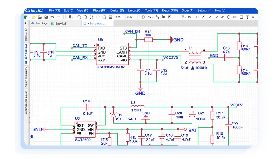
EasyEDA Design Interface
EasyEDA stands out as an accessible, cloud-based electronic design automation (EDA) tool, ideal for both novice and experienced users. This section provides a clear pathway for beginners to initiate their journey with EasyEDA, emphasizing the straightforward process of creating an account, navigating the intuitive interface, and setting up a first project.
Creating Your EasyEDA Account Begin by visiting the EasyEDA website. Locate and click on the 'Sign Up' or 'Register' button. Follow the prompts, providing the necessary information such as your email address, username, and password. Upon completion, you will have successfully created your free EasyEDA account.
Navigating the User Interface Once logged in, you will be presented with the main dashboard. The interface is divided into logical sections, including a project panel, a schematic editor, a PCB layout editor, and a library browser. Familiarize yourself with the layout, as this will be your primary workspace.
Setting Up Your First Design Project To begin a new project, locate the 'New Project' button, usually found in the project panel. Give your project a descriptive name, select a category, and configure the project's settings, if necessary. Upon creation, you will be redirected to an empty schematic sheet, where you will start building your first design.
Schematic Design in EasyEDA: Building Your Circuit
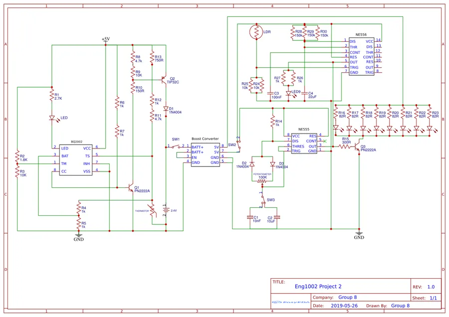
EasyEDA Schematic
EasyEDA's schematic capture tools provide an intuitive environment for constructing electronic circuit diagrams. This process involves selecting components from an extensive library, placing them onto the design canvas, and connecting them using wires to represent electrical pathways. Careful attention to component selection, wiring accuracy, and the incorporation of annotations are crucial for a well-structured and easily understandable schematic.
The schematic serves as a blueprint for the physical PCB layout. Therefore, accurate representation is paramount. This section will guide you through the process, providing the essential knowledge required for effective schematic design in EasyEDA.
Component Library Access EasyEDA offers a vast component library accessible through the 'Library' panel. Components are categorized for easy navigation. Search functionality assists in quickly locating specific parts. Utilize the component preview to verify the symbol before placement.
Component Placement Components are placed onto the schematic canvas via simple drag-and-drop functionality or by using the 'Place' tool. Upon placement, component properties such as the reference designator can be modified. Accurate placement is paramount to avoid overlapping and maintain design clarity.
Wiring and Connections The 'Wire' tool is used to create electrical connections between component terminals. Click-to-connect functionality enables the creation of direct wires. Ensure that wires connect accurately to designated terminals, avoiding unintended connections. A connection dot indicates a proper intersection.
Annotation and Labeling Annotate components with clear reference designators (e.g., R1, C2) using the 'Annotation' tool. Nets should be labeled clearly using the 'Net Label' tool. This ensures that signals are easily identified and tracked throughout the design process. Annotations contribute significantly to the readability and maintainability of the schematic.
Error Checking EasyEDA incorporates an error-checking mechanism to help identify common schematic design errors. Use the 'Design Manager' to look for unconnected terminals, duplicate component IDs, or other issues. Employ these checks to ensure a clean schematic before proceeding to layout.
Circuit Simulation with EasyEDA: Testing Your Design
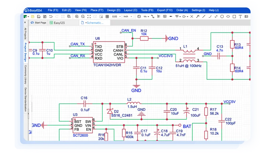
EasyEDA Simulation
EasyEDA's integrated circuit simulator is a powerful tool that allows users to verify the functionality and performance of their electronic designs before physical prototyping. This feature supports various types of analyses, from basic DC and transient simulations to more complex analyses, enabling thorough testing and validation of circuit behavior. By simulating circuits, users can identify potential issues, optimize their designs, and ensure that the final product meets the desired specifications.
The circuit simulator in EasyEDA is an essential component of the design process, allowing for the analysis of key performance indicators, and providing a robust environment for circuit design and validation. It facilitates a more efficient and cost-effective workflow by minimizing errors that could otherwise arise during physical prototyping.
Key aspects of using the EasyEDA circuit simulator include:
DC Analysis Performs a steady-state analysis of the circuit, calculating voltages and currents under static conditions. This is useful for checking bias points and quiescent operating conditions. This helps confirm that the circuit is set up correctly.
Transient Analysis Simulates the circuit's behavior over time, allowing users to observe dynamic responses to time-varying inputs. This is critical for testing the stability and dynamic response of circuits, particularly for designs with filters, oscillators, or control loops. It reveals how the circuit responds to changes, ensuring that it operates as required.
AC Analysis Analyzes the frequency response of the circuit, crucial for understanding how the circuit behaves at different frequencies. This analysis allows designers to identify resonant frequencies, bandwidth, and gain characteristics, vital for circuits such as filters and amplifiers. Analyzing circuits in this way ensure they perform adequately for their intended purpose.
Key Performance Metrics Identify essential parameters such as voltage levels, current consumption, signal distortion, and frequency response. Accurately interpreting these results is crucial for making well-informed design decisions. A well-understood interpretation will allow for informed design decisions.
Debugging Common Errors Address typical errors such as incorrect connections, component value mismatches, and simulation setup issues. Proper debugging techniques can significantly reduce iteration time. Addressing these errors during the design phase ensures a successful final product.
PCB Layout Design in EasyEDA: From Schematic to Physical Board
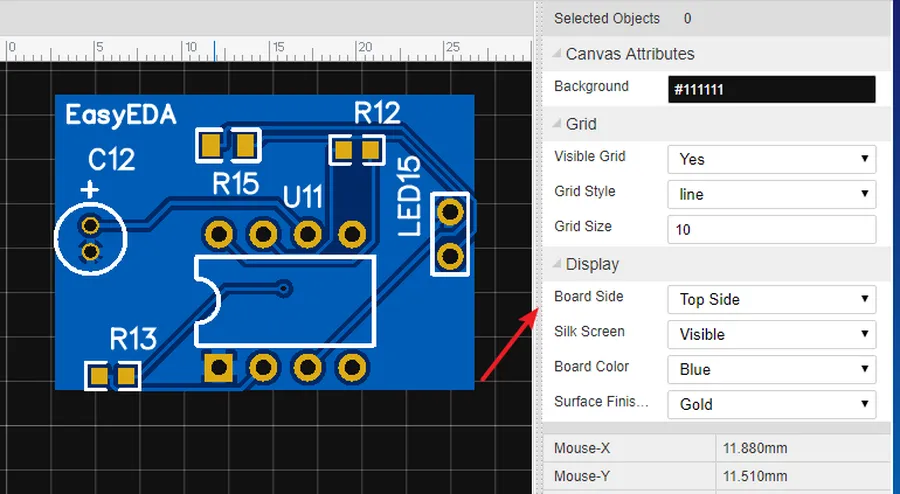
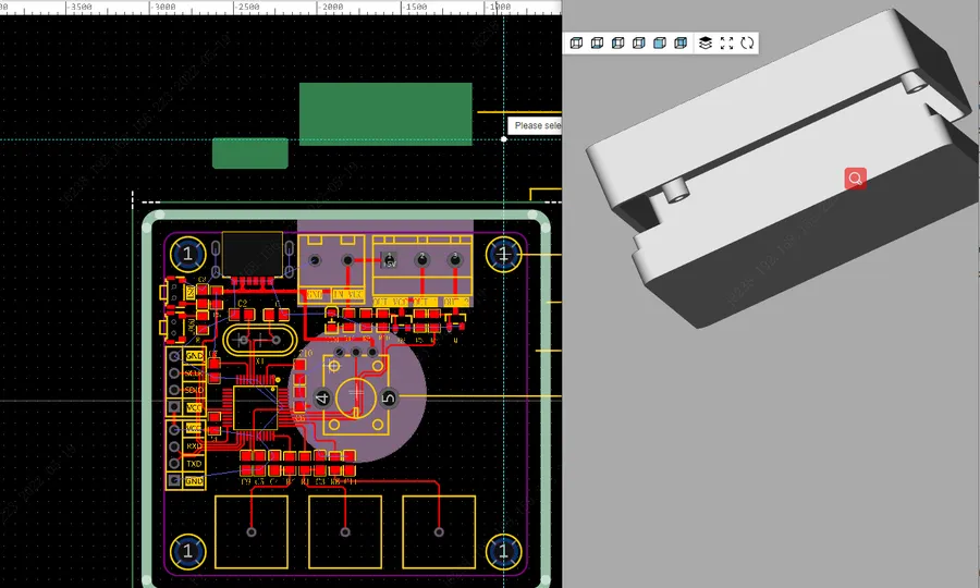
EasyEDA PCB Layout
Transforming a schematic design into a physical printed circuit board (PCB) layout is a crucial step in the electronic design process, and EasyEDA provides a robust suite of tools to facilitate this. The process involves translating the logical connections of your circuit into a physical arrangement of components and conductive pathways on a PCB.
This section will guide you through the essential steps, starting from importing your schematic to generating the necessary files for manufacturing.
Importing the Schematic: Begin by ensuring your schematic is complete and error-free. In EasyEDA, select 'Convert to PCB' to initiate the PCB layout process. The software automatically transfers all components and their connectivity information from the schematic.
Component Placement: Strategically place components on the PCB workspace. Consider factors such as signal flow, thermal management, and physical constraints. EasyEDA allows for both manual placement and automatic arrangement to aid this process. Component placement optimization is critical for minimizing routing complexity.
Setting PCB Design Rules: Before routing traces, configure design rule settings in EasyEDA. Specify track widths, clearances, and via sizes appropriate for your design. This step is vital for ensuring manufacturability and reliability.
Routing Traces: The next step is establishing the electrical connections between the components by drawing conductive tracks on the PCB layers. EasyEDA offers several routing options, including manual routing, auto-routing, and interactive routing. The auto-router is suitable for simple designs, while manual routing offers fine control for more complex boards. Careful routing minimizes signal interference and ensures impedance control.
Design Rule Check (DRC): After routing, run a DRC to identify and correct any violations. This includes track-to-track, track-to-pad, and hole-to-hole clearances. Addressing DRC issues ensures that the final board is manufacturable. EasyEDA flags the errors for user correction.
Adding Ground Planes: Include a ground plane on one or more layers to provide a reference point and improve signal integrity. A ground plane can also assist with heat dissipation and reducing electromagnetic interference. EasyEDA allows you to create both solid and hatched ground planes.
Final Review: Before exporting for manufacturing, meticulously review your PCB layout. Check component placement, routing, and clearances. Verify that all connections are correct. Conduct a visual inspection and use the 3D preview feature to catch any oversights.
Aspect
Description
Component Placement
Strategic arrangement of parts on the PCB.
Routing
Drawing conductive tracks to connect components.
Design Rule Check
Verifying compliance with design constraints.
Ground Planes
Continuous conductive area for signal integrity.
Mastering these steps is fundamental to creating functional and reliable PCB designs in EasyEDA. Each step requires careful attention and adherence to industry best practices to minimize rework, reduce costs and ensure proper performance.
EasyEDA vs. KiCad and Other EDA Tools: A Comparative Analysis
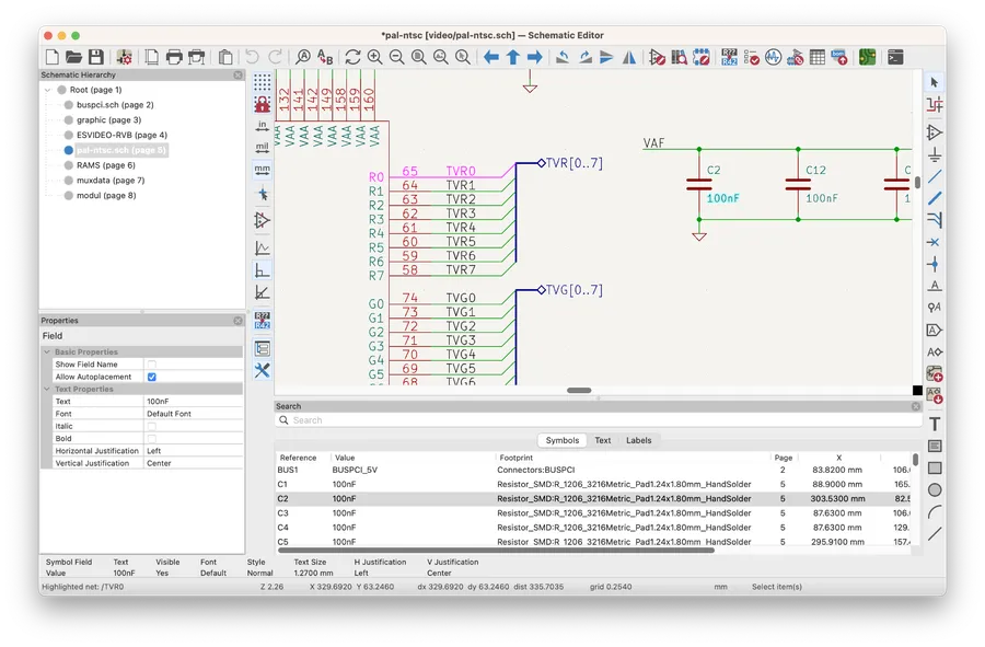
KiCad Interface
Selecting the right Electronic Design Automation (EDA) software is crucial for efficient and effective PCB design. This section provides a comparative analysis of EasyEDA with other popular tools, notably KiCad, to aid users in making informed decisions based on their specific project needs, technical skills, and resource constraints. We will delve into aspects such as user interface, functionality, community support, pricing models, and overall ease of use.
Feature
EasyEDA
KiCad
Other EDA Tools (e.g., Altium Designer, Eagle)
User Interface
Web-based, intuitive, modern look
Desktop application, more traditional interface
Varies; often more complex, with steeper learning curve
Functionality
Good for basic to intermediate designs; integrated with JLCPCB
Comprehensive feature set; suitable for complex designs
Feature-rich; often includes advanced simulation, routing, and collaborative features
Community Support
Active online community; tutorials and forum support
Large and active community; extensive documentation
Varied; depends on the specific tool
Price
Free version with limitations; Pro version available
Completely free and open source
Often paid licenses; prices can be very high
Ease of Use
Very beginner-friendly; simple for quick designs
Moderate learning curve; may take time to master
Steep learning curve; extensive training may be necessary
Cloud/Local
Primarily cloud-based, with option to export files
Local desktop application
Primarily local desktop application
Collaboration
Real-time collaboration features available
More limited collaborative functions
Varied; some have strong collaboration features
Component Library
Large component library, regularly updated
Extensive library, continuously growing
Often well-populated, but may depend on vendor
Simulation
Basic built-in simulator
Basic built-in simulator and possible integration with other simulation tools
Advanced simulation features, offering a wide range of analysis options
EasyEDA's primary strengths lie in its ease of use and seamless integration with JLCPCB, making it an ideal choice for rapid prototyping and smaller projects. KiCad, on the other hand, provides a more robust and professional environment, suitable for complex projects that require more advanced functionality and features. The other EDA tools, while having more functionalities, are often expensive and harder to master. Ultimately, the best choice depends on the user's experience level, project complexity, budget, and desired degree of functionality.
EasyEDA Pro vs. Free Version: Key Differences and Feature Analysis
EasyEDA Pro
EasyEDA offers both a free version and a paid 'Pro' version, each catering to different user needs and project complexities. The core functionality of schematic capture and PCB layout is available in both, but the Pro version unlocks advanced features designed for professional-level design and manufacturing workflows. Understanding these differences is crucial for users to select the appropriate version.
Feature
Free Version
Pro Version
Number of Private Projects
Limited
Unlimited
Number of Public Projects
Unlimited
Unlimited
Advanced Simulation
Basic
Advanced (e.g., SPICE Simulation)
Import and Export Formats
Limited
Extended file format support
Team Collaboration Features
Limited
Enhanced project sharing and access control
Access to Components Libraries
Basic
Extended access
PCB Manufacturing Output Options
Basic
Advanced output options and customization
Customer Support
Community forum
Priority support
Price
Free
Subscription-based
EasyEDA Tips, Tricks, and Hidden Features
EasyEDA, while user-friendly, contains a wealth of advanced functionalities that can significantly enhance user productivity and design precision. This section delves into those lesser-known tips and tricks, aimed at empowering users to leverage EasyEDA to its fullest potential, beyond the basic operations.
Keyboard Shortcuts for Efficiency Mastering keyboard shortcuts significantly speeds up the design process. EasyEDA provides numerous shortcuts for actions like panning (Space + Drag), zooming (Ctrl + Mouse Wheel), rotating components (R), and duplicating selections (Ctrl + D). Utilizing these shortcuts minimizes mouse travel and maximizes efficiency.
Custom Component Libraries and Templates Create custom component libraries from frequently used parts to avoid repetitive searches. Develop templates for common circuit blocks or PCB layouts to rapidly initiate new projects. This also ensures consistency across designs and enhances workflow.
Advanced Selection Filters Employ advanced selection filters to select components based on attributes, improving efficiency in complex designs. For example, select all resistors of a specific value or all components within a specified area by using filter options.
Utilizing the Version Control System Take advantage of EasyEDA's integrated version control system to manage design iterations effectively. Save designs at specific milestones, enabling easy rollback to earlier versions in case of errors or changes.
The Power of the Scripting API EasyEDA exposes a scripting API that permits users to automate tasks and personalize the software. Develop custom scripts to modify design elements or perform intricate tasks repetitively.
Interactive Routing Features Utilize interactive routing features for better trace placement. These tools intelligently adjust traces based on design rules, including auto-push and hug modes, which automatically route the traces and optimize them.
Component Annotation for Enhanced Clarity Use EasyEDA’s annotation tool to systematically identify the values and reference designators. It's advantageous for generating BOMs and is crucial when manufacturing PCBs.
Frequently Asked Questions About EasyEDA
This section addresses common queries regarding EasyEDA, offering clarity on aspects such as its pricing model, accessibility, compatibility, and collaborative features. We delve into the distinctions between the free and pro versions, and offer guidance for users seeking the optimal PCB design software for their needs.
Is EasyEDA software free? Yes, EasyEDA offers a free version that provides a comprehensive suite of tools for schematic capture, PCB layout, and circuit simulation. This free tier is suitable for hobbyists, students, and small-scale projects. Certain advanced features and capabilities, however, are reserved for the paid 'Pro' version.
Is EasyEDA Standard (STD) free? The term 'EasyEDA Standard' typically refers to the free tier of EasyEDA's online platform. Yes, the standard version is free for use, offering a robust set of features sufficient for many users. There is no separate 'EasyEDA STD' product that is different from the standard free offering.
Which is the best free PCB design software? The 'best' software is subjective and depends on individual needs and experience. However, EasyEDA is often cited as a strong contender for best free PCB design software due to its intuitive interface, cloud-based accessibility, and integrated features for schematic capture, PCB layout, and simulation. KiCad is another popular and powerful open-source alternative. Ultimately, the ideal choice depends on user preference, project complexity, and workflow.
What is the difference between EasyEDA and EasyEDA Pro? EasyEDA Pro is the paid version of EasyEDA, offering advanced features not available in the free tier. These include more simulation capabilities, such as more complex analyses and larger simulation component counts, access to more extensive component libraries, and enhanced collaboration features. The Pro version may also offer faster processing speeds and priority support. The free version is designed for basic and medium complexity projects, while EasyEDA Pro is aimed at professional users who require advanced functionality.
Does EasyEDA offer offline access? EasyEDA primarily operates as a cloud-based platform, meaning it requires an internet connection to function. It does not offer a native offline mode for design work. However, users can download their projects as local files for backups or for use with other software.
What file formats does EasyEDA support for import and export? EasyEDA supports a wide variety of file formats for both import and export, including Gerber files for PCB manufacturing, .SVG and .DXF for graphical import/export, and .JSON files for project backup and sharing. It also supports importing of files from other EDA software, such as KiCad and Altium, but with some limitations. The specific file formats supported may vary depending on the task, such as importing components or exporting a PCB layout.
Can I collaborate with others on EasyEDA projects? Yes, EasyEDA supports collaborative work, particularly in the Pro version, which provides advanced teamwork features. In the free version, collaboration is possible but may require more manual management. Users can share project files and libraries, but the Pro version offers features such as version control, concurrent editing and enhanced project sharing to better support simultaneous collaboration.
Integrating EasyEDA with PCB Manufacturing Services
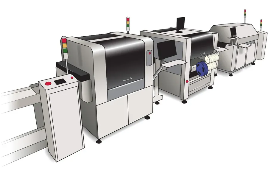
PCB Production Line
Seamlessly transitioning your PCB design from EasyEDA to manufacturing is crucial for bringing your electronic projects to life. This section details the process of exporting your design files, focusing on the necessary settings and file formats required by PCB manufacturers, such as JLCPCB and others, ensuring a smooth production workflow.
Gerber File Generation Gerber files are the industry-standard format for PCB manufacturing. EasyEDA simplifies the process by providing a one-click Gerber generation feature. Ensure that all layers (copper, solder mask, silkscreen, drill) are selected for export. The correct settings are essential to accurate manufacture.
Drill File Generation In addition to Gerber files, a drill file (usually in Excellon format) is essential for defining the locations and sizes of all holes in your PCB. EasyEDA will generate the drill file automatically.
Component Placement File Manufacturers often need a component placement file (a BOM file) that defines the position, rotation, and package type for all components. EasyEDA offers this feature, which is essential for automated assembly. Check that all part numbers and designators are correct.
Manufacturing File Settings Within EasyEDA, configure your export settings to match the specifications of your chosen manufacturer. Common settings include PCB thickness, copper weight, and the minimum trace width, and spacing. This accuracy in settings avoids common production errors.
Exporting for JLCPCB and Other Services EasyEDA is directly integrated with JLCPCB, allowing for a streamlined export process. For other services, use the standard Gerber export and check the service provider's website for specific instructions, making sure the necessary files are there and correctly set up.
Verification and Quality Check Before submitting your files, carefully check your exported Gerber files using a Gerber viewer. This ensures no errors in the generated files, and it mitigates unnecessary manufacturing delays or errors that can be costly, ultimately saving time and money.
EasyEDA stands out as a powerful, accessible, and versatile online tool for PCB design, catering to both beginners and experienced professionals. Its intuitive interface and robust features offer a seamless design process, from initial schematics to final PCB layouts. Whether you're prototyping your next hobby circuit or developing an advanced electronic system, EasyEDA equips you with everything you need to bring your ideas to life. Its integration with JLCPCB also allows for a smooth transition from design to fabrication and assembly, making EasyEDA a comprehensive solution for electronics design needs.