In the fast-paced world of electronic competitions, having a reliable and high-performance development board is crucial for success. The heart of any development board lies in its PCB (Printed Circuit Board), which serves as the foundation for all electronic components and circuitry. A well-designed PCB can significantly impact the board's performance, stability, and overall functionality. This article delves into the critical aspects of PCB solutions for electronic competition development boards, exploring the design considerations, manufacturing processes, and assembly techniques that ensure a competitive edge. Zero One Solution Limited, with its expertise in rapid prototyping and one-stop PCB services, stands ready to empower your innovative solutions.
In the dynamic realm of electronic competitions, where milliseconds can dictate victory or defeat, the Printed Circuit Board (PCB) serves as the bedrock of every high-performance development board. Beyond merely connecting components, the PCB is the invisible architect dictating signal integrity, power distribution, and thermal management, directly impacting the board's speed, reliability, and ultimately, a competitor's success. A poorly designed PCB can introduce noise, degrade signal quality, and lead to thermal bottlenecks, turning a promising design into a frustrating failure. Conversely, a meticulously engineered PCB ensures that the complex interplay of high-speed processors, memory, and sensors operates seamlessly, unlocking the full potential of a development board in the demanding environment of electronic contests.
Designing PCBs for electronic competition development boards demands meticulous attention to several critical factors, as these directly dictate performance, reliability, and ultimately, success in high-stakes environments. Key considerations like signal integrity, robust power distribution, effective thermal management, and strategic component placement are paramount to achieving optimal functionality and stability. Neglecting any of these can lead to signal degradation, power supply issues, overheating, and unreliable operation, all of which are detrimental in competitive electronics.
| Design Aspect | Description | Impact on Performance | Best Practice |
|---|---|---|---|
| Signal Integrity (SI) | Maintaining signal quality and preventing degradation as signals propagate across the PCB. | Ensures accurate data transmission, prevents errors, and allows for higher operating frequencies. | Minimize trace lengths, use controlled impedance routing, employ proper termination. |
| Power Distribution Network (PDN) | Delivering stable and clean power to all components on the board. | Prevents voltage drops, reduces noise, and ensures consistent operation of sensitive ICs. | Utilize wide power and ground planes, strategic decoupling capacitor placement, low-inductance connections. |
| Thermal Management | Dissipating heat generated by components to maintain optimal operating temperatures. | Prevents component damage, improves reliability, and sustains peak performance over extended periods. | Incorporate thermal vias, large copper pours, heat sinks, and consider airflow within the enclosure. |
| Component Placement | Strategic positioning of components to optimize electrical performance and manufacturability. | Minimizes trace lengths, reduces signal coupling, simplifies routing, and aids thermal dissipation. | Place high-speed components close to connectors, separate analog/digital sections, ensure adequate spacing for cooling and rework. |
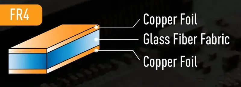
The substrate material forms the backbone of any Printed Circuit Board (PCB), and in high-performance electronic competition development boards, its selection is paramount. The right material dictates crucial electrical and thermal characteristics, directly impacting signal integrity, power efficiency, and the overall reliability of the system under strenuous operational conditions. Choosing an optimal substrate is not merely a design choice; it's a fundamental engineering decision that defines the board's capability to perform at peak levels, especially when dealing with high-speed signals and significant heat dissipation.
| Material Type | Dielectric Constant (Dk) | Dissipation Factor (Df) | Thermal Conductivity | Key Advantages | Typical Applications |
|---|---|---|---|---|---|
| FR-4 | 4.2-4.7 | 0.015-0.025 | 0.2-0.4 W/mK | Cost-effective, widely available, good mechanical strength | General purpose, low-to-moderate frequency boards |
| High-Tg FR-4 | ~4.5 | 0.01-0.015 | 0.3-0.5 W/mK | Improved thermal resistance, better dimensional stability | High-density, moderate-speed digital circuits |
| Rogers (e.g., RO4350B) | 3.48 | 0.0037 | 0.6-0.8 W/mK | Low Dk/Df for high-frequency, excellent thermal stability | RF/Microwave circuits, high-speed data communications, radar |
| PTFE (Teflon) | 2.1-2.3 | 0.0009 | 0.19-0.24 W/mK | Extremely low Dk/Df, excellent high-frequency performance | Ultra-high frequency, aerospace, medical devices |
| Polyimide | 3.0-3.5 | 0.005-0.01 | 0.2-0.3 W/mK | High temperature resistance, good flexibility (for flex PCBs) | Flexible PCBs, high-temperature applications, aerospace |
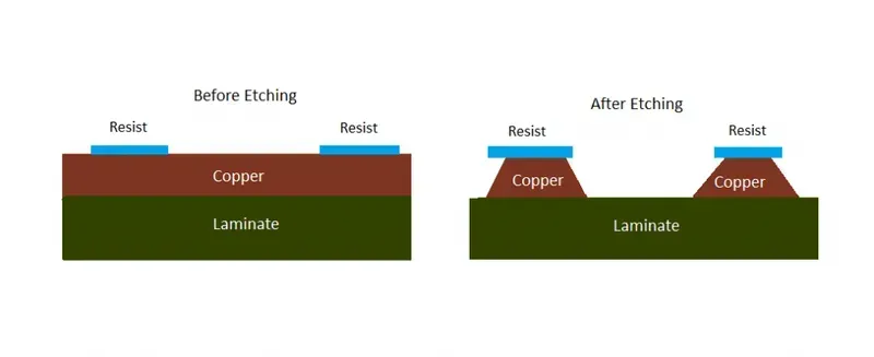
The manufacturing process of Printed Circuit Boards (PCBs) is a highly intricate and critical phase that directly dictates the performance and reliability of electronic competition development boards. Precision and stringent quality control at every stage are paramount to transforming a theoretical design into a functional, robust physical product, capable of withstanding the demanding environments of competitive electronics. From initial material preparation to final surface finishing, each step must adhere to rigorous standards to ensure the longevity and optimal operation of the board.
| Process Step | Description | Precision Criticality | Key Quality Control Focus |
|---|---|---|---|
| Imaging & Etching | Transferring the circuit design onto the copper layers and selectively removing unwanted copper to form traces. | High (Trace width, spacing accuracy) | Uniform etching, no short circuits or open circuits |
| Drilling | Creating precise holes for component leads (through-hole) and vias (interlayer connections). | Very High (Hole diameter, positional accuracy) | Correct hole size, accurate alignment, no burrs |
| Plating (Electroless & Electro) | Depositing copper within the drilled holes and on the surface to create conductive pathways. | High (Copper thickness, uniformity) | Consistent copper thickness, strong adhesion, no voids |
| Solder Mask Application | Applying a protective polymer layer over the copper traces, exposing only component pads for soldering. | Medium (Alignment, coverage) | Even coverage, no mask on pads, no air bubbles |
| Surface Finish Application | Applying a protective metallic coating to exposed copper pads to prevent oxidation and ensure solderability. | High (Thickness, uniformity) | Consistent thickness, good flatness, excellent solderability |
| Profiling/Routing | Cutting the large PCB panel into individual boards according to the specified dimensions. | High (Dimensional accuracy) | Accurate board dimensions, smooth edges, no delamination |
| Electrical Testing (E-Test) | Verifying the continuity of all traces and isolating any short or open circuits. | Very High (Fault detection) | 100% circuit integrity, no electrical defects |
void setup() {
  // Initialize competition board components
  pinMode(LED_BUILTIN, OUTPUT);
  Serial.begin(115200);
}

void loop() {
  // Simulate a competitive task
  digitalWrite(LED_BUILTIN, HIGH);
  delay(100);
  digitalWrite(LED_BUILTIN, LOW);
  delay(100);
  Serial.println("Board operating...");
}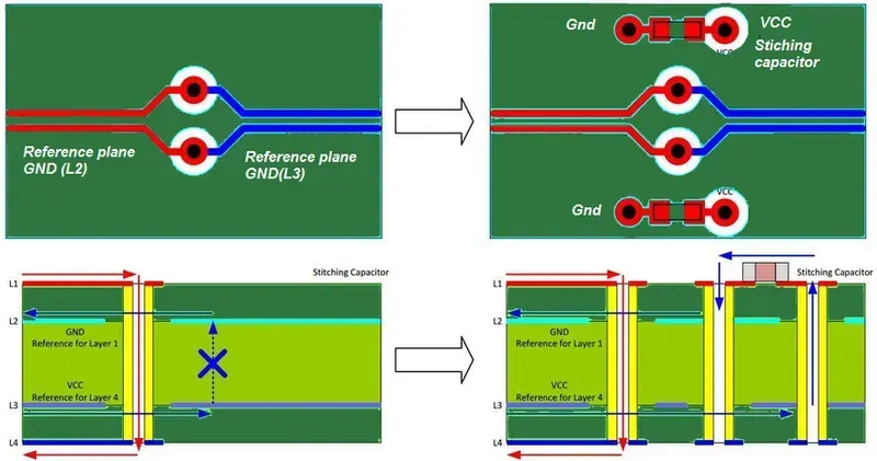
In the realm of electronic competition development boards, achieving optimal signal integrity is paramount for reliable and high-performance operation. High-speed PCB layout techniques are not merely best practices; they are critical engineering disciplines that directly impact the board's ability to transmit data accurately and efficiently. Without meticulous attention to these techniques, even the most sophisticated designs can succumb to signal degradation, leading to unreliable performance and competitive disadvantages. This section delves into the fundamental strategies employed to preserve signal integrity in high-speed PCB designs.
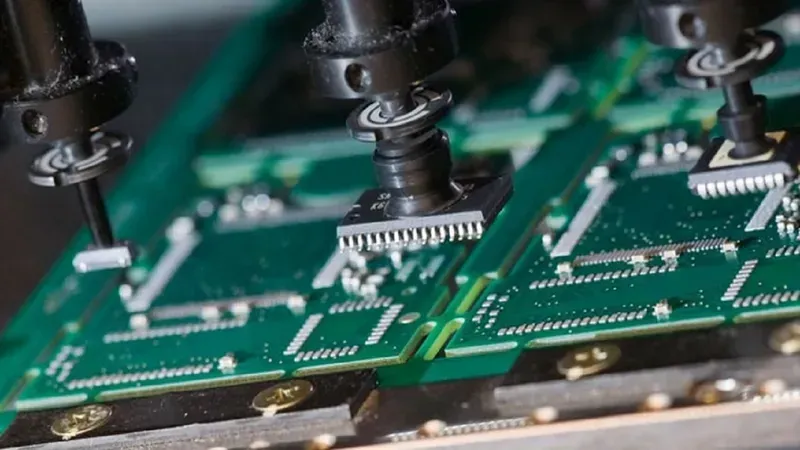
Precise and reliable component assembly is paramount for the functionality and longevity of Electronic Competition Development Boards. The choice between Surface Mount Technology (SMT) and Through-Hole Technology (THT) significantly impacts board density, performance, and manufacturing efficiency. As veteran engineers, we understand that selecting the appropriate assembly method, or a hybrid approach, is critical for achieving optimal circuit performance, especially in high-frequency and high-density electronic competition applications. This decision directly influences the board's form factor, cost-effectiveness, and overall robustness, ensuring it can withstand the rigors of competitive environments.
| Feature | Surface Mount Technology (SMT) | Through-Hole Technology (THT) |
|---|---|---|
| Component Size | Smaller, lighter components | Larger, bulkier components |
| Mounting Method | Components soldered directly onto the PCB surface | Component leads inserted through holes and soldered on the opposite side |
| Board Density | Higher component density, allowing for more compact designs | Lower component density, requires more PCB real estate |
| Automation | Highly automatable, suitable for high-volume production | Often requires manual insertion, less automatable |
| Performance (High Freq.) | Reduced lead inductance/capacitance, better for high-frequency signals | Longer leads introduce more parasitic effects, less ideal for high-frequency |
| Mechanical Strength | Less mechanical strength against vibrations and impacts without additional reinforcement | Higher mechanical strength, more robust connections |
| Cost | Lower cost per component in high volume; higher initial setup costs | Higher cost per component; lower initial setup costs |
| Repairability | More challenging to repair/rework due to smaller components and higher density | Easier to inspect, repair, and replace components |
At Zero One Solution Limited, our state-of-the-art facilities are equipped to handle both SMT and THT assembly with exceptional precision. Our automated SMT lines ensure rapid, high-volume assembly of miniature components, crucial for compact and high-performance electronic competition boards. Concurrently, our expert technicians adeptly handle THT assembly for components requiring superior mechanical stability or for specific power applications. We meticulously manage solder paste application, component placement accuracy, reflow soldering profiles, and wave soldering processes to guarantee robust and reliable connections, meeting the demanding specifications of competitive electronic systems.
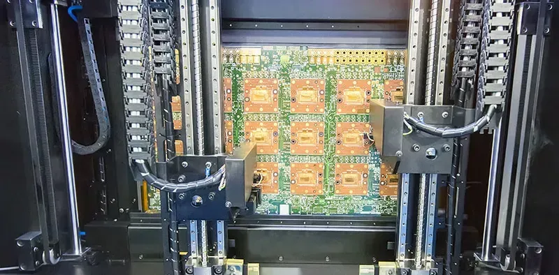
For Electronic Competition Development Boards, rigorous testing and validation are not merely a final step but a crucial continuum ensuring that every PCB functions as intended, withstands operational demands, and delivers peak performance under competitive pressure. This meticulous process safeguards signal integrity, power delivery, and thermal stability, transforming theoretical designs into reliable, high-performing hardware platforms ready for the intense demands of electronic competitions.
| Testing Type | Purpose | Key Parameters Evaluated | Industry Relevance | |
|---|---|---|---|---|
| Electrical Testing (e.g., Flying Probe, Bed of Nails) | Verify circuit continuity, shorts, opens, and component presence. | Resistance, capacitance, inductance, open circuits, short circuits. | IPC-9252 (Electrical Test Guidelines for Bare Boards), IPC-A-600 (Acceptability of PCBs). Essential for validating basic circuit integrity before assembly. | This ensures the fundamental electrical pathways are correct, preventing immediate failures upon power-up. |
| Testing Type | Purpose | Key Parameters Evaluated | Industry Relevance | |
|---|---|---|---|---|
| Signal Integrity (SI) Testing | Assess signal quality at high speeds, minimizing distortion and crosstalk. | Eye diagrams, rise/fall times, overshoot/undershoot, impedance matching, crosstalk noise. | IEEE 802.3 standards for Ethernet, JEDEC standards for memory interfaces. Crucial for high-speed data transmission in competitive electronics. | Critical for boards with DDR, PCIe, or high-speed communication interfaces to ensure data reliability and speed. |
| Testing Type | Purpose | Key Parameters Evaluated | Industry Relevance | |
|---|---|---|---|---|
| Thermal Testing (e.g., Thermal Imaging, Environmental Chambers) | Evaluate heat dissipation efficiency and component temperature under operational loads. | Component temperatures, thermal hotspots, temperature gradients, cooling effectiveness. | JEDEC JESD51 (Thermal Characterization of Integrated Circuits), MIL-STD-810 (Environmental Engineering Considerations). Vital for long-term reliability and preventing performance degradation due to overheating. | Ensures the board remains within safe operating temperatures, preventing thermal throttling and component damage during intense use. |
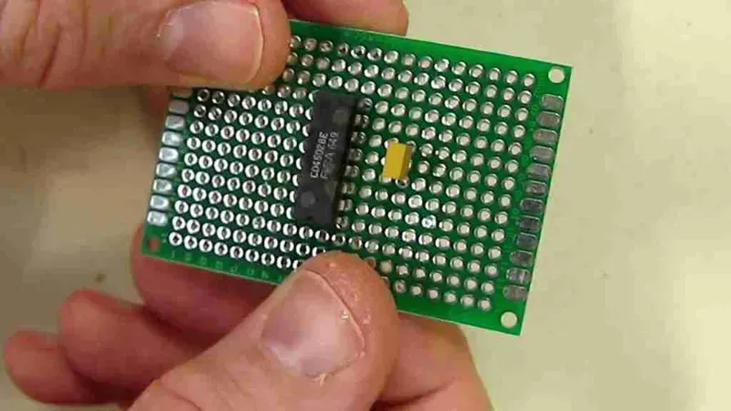
In the fast-paced realm of electronic competitions, where every millisecond and every micron of precision counts, the underlying PCB is not merely a component but a critical enabler of victory. Zero One Solution Limited stands as a premier partner, offering unparalleled rapid prototyping and comprehensive one-stop PCB services specifically tailored for the demanding requirements of electronic competition development boards. Our expertise ensures that your innovative designs are translated into robust, high-performance hardware, giving you the competitive edge.
Navigating the complexities of PCB design and manufacturing for electronic competition development boards can raise numerous questions for engineers and developers alike. This FAQ section addresses the most common inquiries, providing authoritative answers to clarify critical aspects of ensuring optimal performance, reliability, and competitive advantage through superior PCB solutions.
In conclusion, a robust PCB solution is paramount for creating a successful electronic competition development board. From careful design considerations to precise manufacturing and assembly, every step plays a crucial role in optimizing performance and reliability. Zero One Solution Limited is dedicated to providing comprehensive PCB solutions, enabling you to push the boundaries of innovation and achieve excellence in electronic competitions. Contact us today to discover how our expertise can elevate your next project and bring your winning ideas to life. Visit our website or reach out to our team to learn more about our services and how we can help you succeed.

