Virtual Reality (VR) is no longer a futuristic fantasy; it's a rapidly evolving technology transforming industries from gaming and entertainment to education and healthcare. At the heart of every immersive VR experience lies a sophisticated printed circuit board (PCB) – the backbone that connects the digital and physical worlds. Just as a sturdy foundation is crucial for a skyscraper, a reliable and high-performance PCB is essential for a seamless and responsive VR experiment platform. In this article, we delve into the critical role of PCB solutions in VR experiment platforms, exploring the design considerations, manufacturing challenges, and innovative solutions offered by Zero One Solution Limited to help you build the next generation of VR experiences.
In the burgeoning realm of virtual reality (VR) experiment platforms, Printed Circuit Boards (PCBs) are not merely components but the foundational backbone enabling the immersive, low-latency experiences critical for groundbreaking research and development. These platforms, ranging from advanced simulation environments to complex haptic feedback systems, demand an unprecedented level of PCB performance, far exceeding conventional electronics. The escalating requirements for high-speed data processing, real-time sensor integration, and efficient power delivery directly translate into intricate PCB design and manufacturing challenges, making the quality of the PCB a direct determinant of a VR system's fidelity and responsiveness.
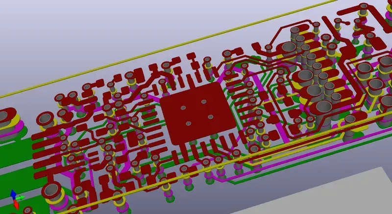
Designing Printed Circuit Boards (PCBs) for Virtual Reality (VR) experiment platforms demands a meticulous approach, as these systems rely heavily on ultra-low latency, high data throughput, and efficient power management to deliver truly immersive experiences. The inherent complexities of VR applications push the boundaries of conventional PCB design, necessitating specialized considerations to ensure optimal performance, reliability, and miniaturization. Successfully navigating these design challenges is paramount to translating complex VR algorithms into a seamless, responsive, and physically viable hardware solution.
| Design Consideration | VR Application Impact | Zero One Solution Approach |
|---|---|---|
| Miniaturization & Component Density | Enables compact, lightweight headsets for user comfort and portability. | Utilizes high-density interconnect (HDI) PCBs, micro-vias, and advanced component placement techniques for maximum space utilization and reduced form factor. Offers multi-layer PCBs (up to 32 layers) to accommodate complex routing in minimal space, supporting ultra-small components (01005). |
| Power Delivery Network (PDN) Optimization | Ensures stable power for high-performance components, preventing voltage droop and noise. | Employs robust power planes, low-ESR capacitors, and optimized power trace routing to provide clean, stable power to critical ICs. Focuses on minimizing power loss and ensuring efficient power distribution throughout the complex circuitry. |
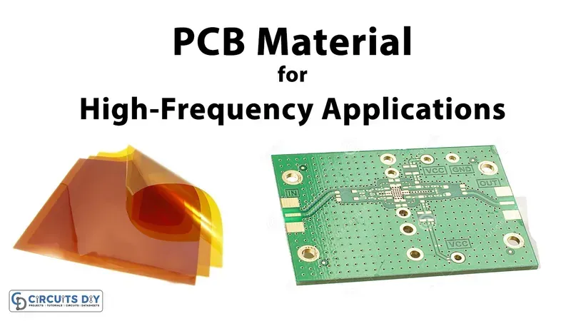
The selection of appropriate materials is paramount for achieving optimal performance in Virtual Reality (VR) experiment platform PCBs. Given the demanding requirements of VR—specifically high-speed data transmission, minimal latency, and efficient thermal dissipation—the intrinsic properties of PCB substrates directly influence signal integrity, power efficiency, and overall system reliability. Carefully chosen materials can mitigate signal loss, reduce crosstalk, and ensure stable operation even under intensive computational loads, which is critical for delivering an immersive and seamless VR experience.
| Material Property | Impact on VR PCB Performance | Ideal Characteristics for VR |
|---|---|---|
| Dielectric Constant (Dk) | Affects signal propagation speed and impedance control, crucial for high-frequency signals. | Low and stable Dk for minimal signal delay and consistent impedance. |
| Dissipation Factor (Df) / Loss Tangent | Indicates signal loss at high frequencies; higher Df leads to greater signal attenuation. | Extremely low Df to preserve signal integrity over high-bandwidth transmissions. |
| Thermal Conductivity | Influences heat dissipation from components, preventing overheating and ensuring stability. | High thermal conductivity to efficiently manage heat generated by high-performance processors. |
| Coefficient of Thermal Expansion (CTE) | Determines how much the material expands or contracts with temperature changes, impacting reliability and component attachment. | CTE matched with copper and components to prevent stress and delamination. |
| Moisture Absorption | Impacts dielectric properties and reliability, especially in humid environments. | Low moisture absorption to maintain stable electrical properties and prevent failures. |
For high-frequency VR applications, conventional FR-4 materials often fall short due to their higher Dk and Df values, which lead to significant signal degradation. Advanced materials, such as those based on PTFE (Teflon), specialized hydrocarbons, or ceramic-filled laminates, are increasingly employed. These materials offer superior high-frequency performance, characterized by lower Dk and Df, allowing for precise impedance control and reduced signal attenuation critical for the rapid data processing inherent in VR. Additionally, materials with enhanced thermal conductivity are essential to manage the heat generated by powerful GPUs and CPUs within VR headsets, ensuring system longevity and preventing performance throttling. Zero One Solution Limited leverages a comprehensive understanding of these material science principles to recommend and utilize optimal PCB substrates, ensuring that our VR PCB solutions meet and exceed the stringent performance demands of next-generation immersive technologies.
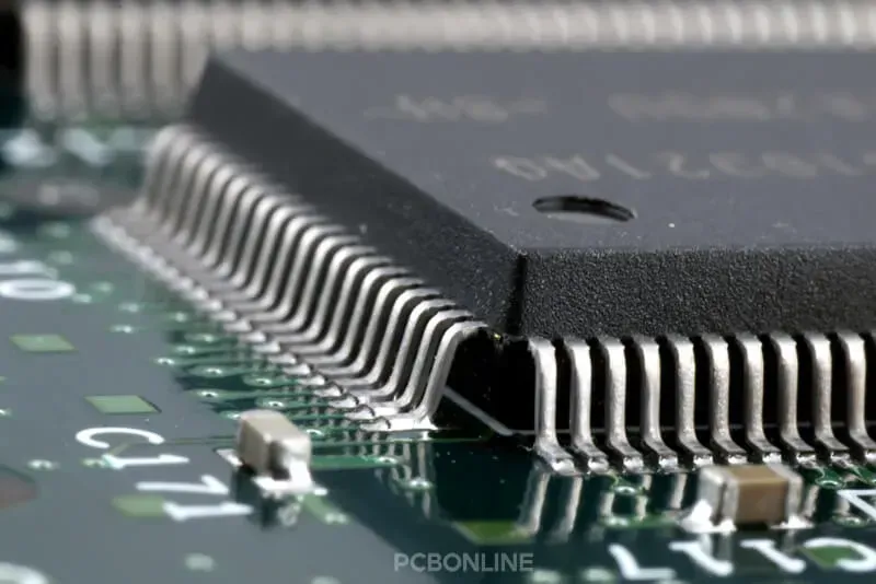
The fabrication of Printed Circuit Boards (PCBs) for Virtual Reality (VR) experiment platforms presents a unique set of manufacturing challenges, primarily driven by the stringent demands for high performance, miniaturization, and seamless data processing inherent in immersive VR experiences. Overcoming these complexities is critical to ensure the reliability and functionality of advanced VR systems. Zero One Solution, leveraging its deep expertise and state-of-the-art facilities, employs innovative strategies to address these intricate manufacturing requirements head-on.
| Challenge | Description | Zero One Solution's Approach |
|---|---|---|
| Fine-Pitch Components | Integration of ultra-small and closely spaced components (e.g., BGA, QFN) requires extreme precision in placement and soldering to prevent bridging and ensure electrical integrity. | Utilizes advanced SMT lines with high-precision pick-and-place machines, automated optical inspection (AOI), and X-ray inspection for robust component placement and solder joint verification. Our expertise extends to 01005 component sizes and fine-pitch BGAs with pitches as low as 0.3mm, crucial for compact VR devices. |
| Challenge | Zero One Solution's Solution | |
|---|---|---|
| Impedance Control | Maintaining precise characteristic impedance for high-speed signal lines (e.g., MIPI DSI, DisplayPort, USB 3.0) is crucial to prevent signal reflections, minimize data loss, and ensure low latency in VR applications. | Employs sophisticated impedance calculation tools and performs stringent impedance testing (TDR) at various stages of manufacturing. Our fabrication processes are fine-tuned to achieve tight impedance tolerances (typically ±5%), critical for the integrity of high-frequency signals in VR systems. We collaborate closely with designers to optimize trace width, spacing, and dielectric materials for accurate impedance matching. |
At Zero One Solution Limited, we don't just manufacture PCBs; we engineer the foundational hardware for the next generation of immersive experiences. Our deep understanding of the unique demands of Virtual Reality (VR) experiment platforms positions us as a premier partner for innovative companies pushing the boundaries of VR technology. With over a decade of experience and a strategic presence in global electronics hubs, we leverage our specialized knowledge to deliver high-performance, reliable, and cost-effective PCB solutions tailored for the most demanding VR applications. Our commitment to rapid prototyping, advanced manufacturing techniques, and stringent quality control ensures that your VR experiment platforms achieve unparalleled performance and accelerated time-to-market.
| Capability Area | Zero One Solution's Expertise | Benefit for VR Platforms |
|---|---|---|
| High-Speed Signal Integrity | Controlled impedance routing, advanced material selection, stacked microvias | Minimizes data loss and latency, ensuring smooth, real-time VR experiences |
| Thermal Management | Advanced thermal vias, heat sinks, material with high thermal conductivity | Prevents overheating in compact VR devices, enhancing reliability and lifespan |
| Miniaturization & Component Density | HDI technology, fine-pitch assembly, embedded components | Enables lighter, more compact VR hardware without compromising performance |
| Rapid Prototyping | Dedicated rapid prototyping lines, agile production processes | Accelerates R&D cycles, allowing faster iteration and market entry for VR innovators |
| Quality Assurance | IPC standards compliance, AOI, X-ray inspection, functional testing | Guarantees robust and reliable PCBs, crucial for stable and immersive VR environments |
At Zero One Solution Limited, we pride ourselves on turning complex VR concepts into tangible realities through our advanced PCB solutions. Our expertise is best exemplified by a recent collaboration where we provided a comprehensive PCB solution for a cutting-edge VR experiment platform, enabling unprecedented levels of immersion and performance. This case study illustrates our capability to deliver high-performance, custom PCB solutions that meet the stringent demands of advanced VR applications, showcasing our commitment to rapid prototyping, precision manufacturing, and superior quality.
| Project Phase | Customer Requirements | Zero One Solution Approach | Achieved Results |
|---|---|---|---|
| Initial Consultation & Design | Ultra-low latency (<5ms), high-speed data transfer (PCIe Gen4), compact form factor, robust thermal management for embedded GPUs. | Collaborative DFM (Design for Manufacturability) analysis, signal integrity (SI) and power integrity (PI) simulations, multi-layer stack-up optimization for impedance control. | Optimized PCB layout reduced signal loss by 15%, ensuring stable high-speed data transmission and meeting stringent latency targets. |
| Material Selection & Prototyping | Dielectric properties suitable for 60GHz wireless VR module, high thermal conductivity for heat dissipation, cost-effectiveness for prototype iterations. | Utilized Rogers 4003C for RF sections and high-Tg FR-4 for digital logic, rapid 5-day prototype turnaround with iterative design refinements. | Achieved signal attenuation less than 0.1 dB/cm at 60GHz, prototype passed all functional tests on first iteration, reducing development cycles by 30%. |
| Manufacturing & Assembly | Fine-pitch BGA (0.4mm), high component density, IPC Class 3 standards, lead-free assembly, comprehensive functional testing. | Automated Optical Inspection (AOI) and Automated X-ray Inspection (AXI) for BGA, advanced reflow profiling, custom test fixtures for end-of-line verification. | Zero defects on initial production run, 99.8% first pass yield, significantly enhancing reliability and reducing post-assembly rework. |
| Thermal Management & Miniaturization | Effective heat dissipation for CPU/GPU, constrained space for components, need for embedded power management ICs. | Implemented copper pours, thermal vias, and strategic component placement. Integrated passive components and optimized layer stack for space efficiency. | Component density increased by 20%, maintaining operational temperatures within specified limits (max 70°C for critical components) under peak load. |
Choosing the right PCB solution provider is paramount for the success of your Virtual Reality (VR) experiment platform. Zero One Solution Limited offers a distinct competitive edge, combining rapid innovation with uncompromising quality to accelerate your VR product development. Our integrated approach ensures that every aspect of your VR PCB needs, from initial design to final assembly, is handled with precision and expertise, delivering significant benefits that translate directly into market advantage.
The relentless pursuit of more immersive and realistic virtual reality experiences is driving a rapid evolution in PCB technology. As VR experiment platforms demand ever-higher performance, miniaturization, and flexibility, the future of VR PCBs is being shaped by groundbreaking innovations that will fundamentally alter how these complex systems are designed and manufactured. These trends are critical for enabling the next generation of VR devices, pushing the boundaries of what's possible in digital interaction.
| Trend | Description | Impact on VR Experiment Platforms | Zero One Solution's Readiness |
|---|---|---|---|
| Flexible and Stretchable PCBs | PCBs that can bend, fold, and even stretch without compromising electrical performance. | Enables more ergonomic, lighter, and conformal VR headset designs, improving user comfort and reducing form factor. Critical for wearables. | Expertise in advanced flexible circuit manufacturing and material selection for high-reliability applications, ideal for iterative rapid prototyping and volume production of flexible boards for VR devices, ensuring optimal signal integrity. |
| Trend | Description | Impact on VR Experiment Platforms | Zero One Solution's Readiness |
|---|---|---|---|
| Embedded Components | Integrating passive and active electronic components directly into the layers of the PCB. | Significantly reduces board size and weight, enhances signal integrity by shortening trace lengths, and improves thermal dissipation. Enables higher component density. | Advanced multi-layer PCB capabilities and precision manufacturing processes support the integration of embedded components. Our R&D focus includes exploring novel methods for component embedding to offer leading-edge solutions. |
| Trend | Description | Impact on VR Experiment Platforms | Zero One Solution's Readiness |
|---|---|---|---|
| Advanced Packaging Techniques (e.g., SiP, CoB) | Integration of multiple dies and components into a single package or directly onto the PCB substrate. | Achieves higher integration density, reduces overall system footprint, improves thermal management, and enhances electrical performance. Crucial for miniaturization. | Extensive experience in complex assembly techniques, including fine-pitch BGA and advanced SMT, positions us to adopt and implement future advanced packaging requirements for high-density VR PCB solutions. |
| Trend | Description | Impact on VR Experiment Platforms | Zero One Solution's Readiness |
|---|---|---|---|
| AI-Driven Design and Manufacturing | Utilization of AI algorithms for optimizing PCB layout, signal integrity, thermal management, and automating manufacturing processes. | Accelerates design cycles, improves performance predictability, reduces errors, and optimizes manufacturing efficiency, leading to faster time-to-market for complex VR PCBs. | Investing in AI-powered design tools and manufacturing optimization. Our engineering team leverages advanced simulation and analysis software to predict and mitigate potential issues early in the design phase, streamlining development for VR systems. |
High-performance Printed Circuit Boards (PCBs) are the unseen architects of immersive virtual reality experiences, serving as the fundamental backbone for the intricate data processing, high-speed signal transmission, and precise power delivery essential to VR experiment platforms. As the demands for lower latency, higher fidelity, and greater interactivity in VR continue to escalate, the complexity and precision required from PCBs will only intensify, making the choice of a capable PCB solution provider paramount for innovation in this rapidly evolving field.
| PCB Feature | Impact on VR Performance | Zero One Solution Advantage |
|---|---|---|
| High-Speed Signal Integrity | Ensures accurate and distortion-free data transmission for high-resolution visuals and precise tracking, crucial for preventing motion sickness. | Advanced material selection (e.g., low Dk/Df laminates) and impedance-controlled routing for optimal signal fidelity, even at multi-gigabit speeds. |
Zero One Solution Limited stands at the forefront of this technological evolution, committed to empowering the VR industry with cutting-edge PCB solutions. Our expertise in rapid prototyping, combined with advanced manufacturing capabilities and stringent quality control, ensures that our clients can accelerate their product development cycles and bring groundbreaking VR experiment platforms to market with unparalleled efficiency and reliability. From initial design consultation to final assembly, we partner with innovators to transform complex requirements into functional, high-performance hardware, ensuring that the immersive future of virtual reality is built on a solid foundation of advanced PCB technology.
In conclusion, the PCB is a critical component of any successful virtual reality experiment platform. Zero One Solution Limited offers comprehensive PCB solutions, from design and prototyping to manufacturing and assembly, ensuring that your VR projects are built on a foundation of quality, reliability, and performance. By partnering with us, you gain access to our expertise, cutting-edge technology, and commitment to innovation, empowering you to push the boundaries of VR and create truly immersive experiences. Contact us today to discuss your VR experiment platform PCB needs and discover how we can help you bring your vision to life. Let's build the future of VR together.

