In an increasingly digital world, the electronic signature pad has become an indispensable tool, streamlining transactions and enhancing security across various industries. From retail point-of-sale systems to legal document signing and healthcare applications, these devices rely on robust, high-performance Printed Circuit Boards (PCBs) to function flawlessly. At Zero One Solution Limited, a leader in rapid-response R&D prototype manufacturing since 2011, we understand that the heart of any reliable electronic signature pad lies in its PCB. This article delves into how our specialized PCB solutions empower businesses to develop cutting-edge electronic signature pads, combining efficiency, precision, and unmatched quality.
The proliferation of digital transactions and the escalating need for enhanced data security have propelled electronic signature pads from niche devices to ubiquitous tools across diverse industries. This surge in adoption, driven by the imperative for streamlined workflows and legally binding digital authentication, directly correlates with a critical demand for sophisticated and reliable Printed Circuit Board (PCB) solutions that form the technological backbone of these devices.
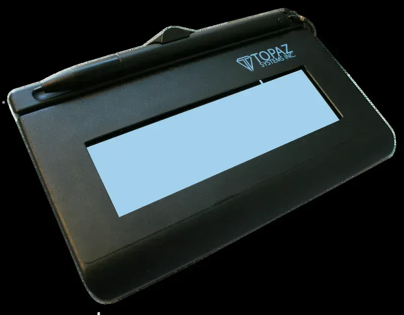
The performance and reliability of an electronic signature pad are intrinsically linked to the sophistication of its Printed Circuit Board (PCB). A robust PCB design for these devices integrates several critical components that work in concert to facilitate accurate signature capture, secure data processing, and efficient power management. Understanding these core components is paramount for any developer seeking to engineer a high-performance electronic signature pad.
| Component Category | Key Components | Functional Requirements | |
|---|---|---|---|
| Processing Unit | Microcontroller (MCU) | High-speed processing, low power consumption, secure data handling, cryptographic capabilities (e.g., ARM Cortex-M series). | |
| Input Interface | Digitizer/Touch Controller, Pressure Sensors | Precise capture of pen input (position, pressure, tilt), high sampling rate, low latency, robust to environmental factors. Examples include Wacom's EMR technology or resistive/capacitive touch controllers like Atmel's maXTouch series for multi-touch and stylus input on display integration. Sensor types could include force-sensing resistors (FSRs) or strain gauges for pressure sensitivity, often integrated within the digitizer layer itself. Digital transformation requires these to be highly accurate and responsive, with resolutions often exceeding 2000 LPI (Lines Per Inch) to capture minute details of a signature for biometric analysis or forensic verification. Specialized ASIC (Application-Specific Integrated Circuit) or FPGA (Field-Programmable Gate Array) solutions may be employed for high-speed signal processing and noise reduction from the digitizer's raw data, crucial for maintaining signature fidelity and preventing data loss during rapid pen movements. Furthermore, the selection of the digitizer should consider the display technology used, ensuring seamless integration between the input and output layers for a natural signing experience. Advanced algorithms for anti-aliasing and trajectory prediction are often implemented in the microcontroller or dedicated co-processor to enhance the visual representation of the signature on the display, making it appear smooth and continuous even with fast strokes. The digitizer interface is also critical for supporting various stylus types, from passive to active pens, each with specific electrical characteristics and communication protocols (e.g., AES protocol for active pens). | |
| Display Interface | LCD/OLED Driver IC, Graphics Controller | Support for various display technologies (e.g., TFT LCD, OLED), high resolution and color depth, fast refresh rates for real-time ink display, robust communication protocols (e.g., MIPI DSI, LVDS). | |
| Memory | Flash Memory, RAM (SRAM/DRAM) | Secure storage for firmware, captured signatures, and application data; sufficient RAM for real-time processing and buffer. For secure data storage, eMMC (embedded MultiMediaCard) or UFS (Universal Flash Storage) solutions are often preferred due to their integrated controller and enhanced reliability compared to raw NAND flash. In addition, secure elements (SEs) or Trusted Platform Modules (TPMs) are frequently incorporated to protect cryptographic keys and sensitive user data, ensuring compliance with data privacy regulations like GDPR and CCPA. The type and size of memory are critical for supporting features such as offline signature capture, where signatures can be temporarily stored on the device before being uploaded to a backend system. Error-correcting code (ECC) memory may also be used in high-reliability applications to prevent data corruption. Furthermore, the memory subsystem must be designed to withstand power fluctuations and abrupt shutdowns without data loss, often involving supercapacitors or small backup batteries to ensure critical data is written to non-volatile memory before power failure. This robust memory architecture is fundamental to maintaining data integrity and system stability in demanding operational environments, especially in high-transaction environments where data loss is unacceptable and can lead to significant financial or legal repercussions. Effective memory management also includes wear-leveling algorithms for flash memory to extend its lifespan, a crucial consideration for devices expected to have a long operational life with frequent write cycles, such as signature pads used for high-volume transactions. The integration of advanced encryption standards (AES) directly into the memory controller or microcontroller also contributes to data security, providing hardware-level protection against unauthorized access. This multi-layered approach to memory design, from type selection to integrated security features, underscores its role as a cornerstone of a secure and reliable electronic signature pad system, facilitating both performance and compliance requirements for sensitive data handling, while ensuring the device's operational longevity and data integrity in diverse application scenarios requiring secure data logging and retrieval, critical for auditing and legal verification processes in financial, retail, and healthcare sectors, where the authenticity and non-repudiation of signatures are paramount. This holistic approach ensures that the electronic signature pad not only captures but also securely stores and transmits signature data, thereby fulfilling its primary function while adhering to stringent industry regulations and user expectations for privacy and reliability, making it a dependable tool in digital workflows across various industries needing secure data capture and storage for compliance and auditing purposes, where data integrity is not just a feature but a fundamental requirement for legal and operational validity. It's imperative that the memory solution supports fast boot times and rapid data access, enabling a seamless user experience, which is especially important in high-volume transaction environments where delays can impact efficiency and customer satisfaction. The choice between volatile and non-volatile memory, alongside the implementation of error correction and data encryption, forms the backbone of a robust and secure electronic signature pad, ensuring that the device can reliably perform its duties in sensitive data environments, adhering to the highest standards of data security and operational efficiency, thereby providing a secure and reliable platform for digital signature capture that meets both performance and compliance demands in a wide range of applications, from retail POS to medical consent forms. This foundational memory infrastructure is critical for the overall system integrity and user trust, providing a solid base for the sophisticated functionalities required in modern digital signature solutions, while also ensuring the longevity and reliability of the device in continuous use environments. Furthermore, efficient memory partitioning and management are essential to optimize system performance and security, separating sensitive data from application code and ensuring that system resources are allocated effectively to prevent performance bottlenecks. The integration of secure boot mechanisms, which verify the integrity of the firmware stored in flash memory, adds another layer of security, protecting against malicious tampering and unauthorized software modifications. These advanced memory management and security features are crucial for building trust in electronic signature pads as reliable and secure devices for critical data capture and processing, a key differentiator in a competitive market. Moreover, the selection of memory components must consider their power consumption characteristics, especially for battery-powered signature pads, to maximize device autonomy and minimize the need for frequent recharging, contributing to overall user convenience and operational efficiency, thereby enhancing the product's market appeal and user adoption rates. The ability to perform firmware over-the-air (FOTA) updates securely is also dependent on the memory architecture, allowing for continuous improvements and security patches without requiring physical device access, thereby reducing maintenance costs and extending the device's operational lifespan. This comprehensive approach to memory selection and integration is vital for delivering a high-quality, secure, and future-proof electronic signature pad solution, meeting the evolving demands of digital transformation and cybersecurity threats, positioning the product as a reliable and innovative solution for modern businesses. The choice of memory also impacts the device's ability to handle complex graphical user interfaces (GUIs) and real-time processing of signature data, requiring sufficient bandwidth and low latency to ensure a smooth and responsive user experience, which is paramount for user satisfaction and adoption of digital signing workflows. Finally, the memory must be resilient to environmental factors such as temperature and humidity, especially for devices deployed in diverse operational environments, ensuring consistent performance and data integrity under various conditions, thereby contributing to the device's overall robustness and reliability in the field. This meticulous attention to memory design, from performance to security and environmental resilience, underscores its pivotal role in the development of a market-leading electronic signature pad, ensuring it meets the rigorous demands of digital signature capture and processing. The strategic selection and integration of memory components are therefore not just a technical detail but a critical enabler for the signature pad's overall success and utility in sensitive applications. | Robust power delivery, efficient voltage regulation, battery management (for portable devices), overcurrent/overvoltage protection. For battery-powered devices, highly efficient Power Management ICs (PMICs) are crucial to extend battery life, integrating features like dynamic voltage scaling and low-power modes. Fast charging capabilities and robust battery protection circuits (e.g., overcharge, over-discharge, short-circuit protection) are also vital. Power delivery networks (PDNs) on the PCB must be carefully designed to minimize noise and ripple, ensuring stable power to sensitive analog and digital components. This involves proper decoupling capacitor placement and careful trace routing to avoid voltage drops and ground bounce. Additionally, consideration for energy harvesting or low-power wireless charging solutions might be incorporated in advanced designs to enhance user convenience and reduce environmental impact. The power management subsystem also includes power-on reset (POR) and brown-out detection (BOD) circuits to ensure proper system initialization and prevent data corruption during power fluctuations, thereby contributing to the device's overall reliability and data integrity. Furthermore, thermal management strategies, such as heat sinks or thermal vias, may be necessary for components that generate significant heat, to maintain optimal operating temperatures and extend component lifespan. The efficiency of the power conversion stages (e.g., buck/boost converters) is also critical, especially in portable devices, to minimize energy loss and maximize battery runtime. Integration of USB Power Delivery (USB-PD) standards allows for flexible and rapid charging, as well as enabling the device to be powered directly from a host device. Effective power management is not just about extending battery life but also about ensuring stable operation and protecting the sensitive electronics within the signature pad from electrical stresses, making it a foundational element of the device's long-term reliability and performance. This comprehensive approach to power management ensures that the electronic signature pad operates consistently and reliably under various power conditions, from battery-powered mobile use to continuous desktop operation, thereby enhancing user experience and device longevity. The ability to monitor battery health and provide accurate charge level indications is also a key feature, preventing unexpected shutdowns and improving user confidence in the device's availability. This meticulous attention to power management design is essential for creating a robust and user-friendly electronic signature pad solution. |
Zero One Solution Limited specializes in designing and manufacturing PCBs that flawlessly integrate these complex components. Our expertise ensures signal integrity, optimal power distribution, and compact layouts, which are crucial for the performance and form factor of modern electronic signature pads. We prioritize robust design practices to handle the unique challenges of high-volume signature capture, ensuring both durability and security.
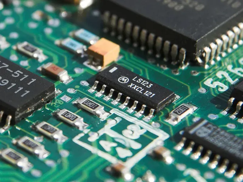
Designing and manufacturing Printed Circuit Boards (PCBs) for electronic signature pads presents a unique set of challenges that demand meticulous attention to detail and advanced engineering expertise. These devices, critical for secure digital transactions, require PCBs that can withstand rigorous usage while maintaining impeccable performance and reliability. The inherent complexities arise from the need to integrate sensitive touch technologies, robust security features, and efficient power management within a compact and durable form factor, all while ensuring compliance with stringent industry standards.
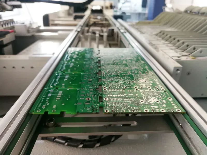
Zero One Solution Limited stands at the forefront of providing bespoke Printed Circuit Board (PCB) solutions for electronic signature pads, leveraging over a decade of specialized experience in rapid prototyping and full-spectrum manufacturing. Our deep understanding of the unique demands of signature pad technology, from precise touch recognition to secure data transmission, enables us to engineer high-performance, compact, and durable PCBs that are critical for the seamless operation and widespread adoption of these devices in diverse sectors.
| Capability Area | Zero One Solution's Advantage | Benefit for Electronic Signature Pad PCBs |
|---|---|---|
| High-Density Interconnect (HDI) | Advanced HDI technology for miniaturization and complex routing. | Enables smaller form factors and higher functionality for sleek signature pads, optimizing board space and component density for superior performance and reduced overall device size, crucial for portable applications and ergonomic designs. |
Our commitment to excellence extends beyond technical capabilities; we foster collaborative partnerships, working closely with clients to understand their specific needs and deliver solutions that not only meet but exceed expectations, positioning Zero One Solution Limited as the preferred partner for advanced electronic signature pad PCB solutions.
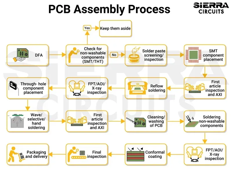
Zero One Solution Limited offers a truly integrated one-stop service for Electronic Signature Pad PCB Solutions, encompassing every phase from conceptual design to final assembly. This comprehensive approach streamlines the entire product development lifecycle, mitigating risks, reducing lead times, and ensuring a cohesive, high-quality end product tailored precisely to the stringent demands of digital signature applications.
| Service Phase | Key Activities | Benefits for Electronic Signature Pads |
|---|---|---|
| PCB Design & Layout | Schematic capture, stack-up definition, component placement, routing optimization, DFM/DFA analysis. | Ensures compact form factors, optimal signal integrity, and manufacturability crucial for reliable signature capture and display. |
| PCB Manufacturing | Material selection, multi-layer fabrication, advanced drilling, surface finish application, impedance control. | Guarantees robust, high-performance boards capable of withstanding continuous use and diverse environmental conditions. |
| Component Sourcing | Global procurement network, counterfeit detection, inventory management, cost optimization. | Secures authentic, high-quality components for displays, sensors, microcontrollers, and power management, critical for device functionality. |
| PCBA (Assembly) | Automated SMT/PTH assembly, fine-pitch placement, BGA rework, functional testing (ICT, FCT). | Delivers fully assembled, tested boards with precise component placement and soldering, ensuring operational readiness and longevity. |
| Quality Assurance & Testing | AOI, X-ray inspection, thermal cycling, environmental testing, burn-in testing. | Verifies compliance with performance standards, ensures reliability and durability, and minimizes post-production failures. |
| Logistics & Delivery | Global shipping, customs clearance, secure packaging, inventory holding options. | Facilitates timely and secure delivery of finished PCBs or assembled units to any global destination. |
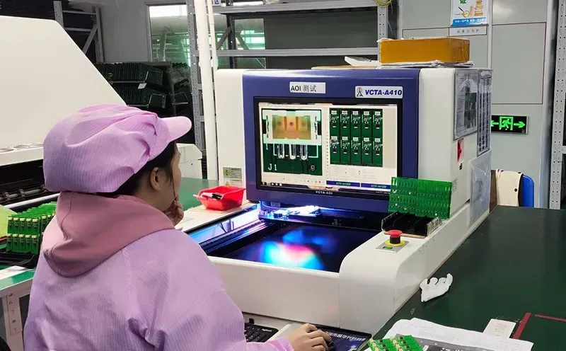
Ensuring the unwavering reliability and performance of Electronic Signature Pad PCBs is paramount, given their critical role in secure digital transactions. At Zero One Solution Limited, our commitment to quality assurance is embedded in every stage of the PCB lifecycle, from initial design verification to final assembly and rigorous testing. We understand that the integrity of an electronic signature relies directly on the robustness and accuracy of its underlying hardware, demanding the most stringent quality control measures to guarantee long-term durability and flawless operation in diverse operational environments.
| Testing Phase | Key Objectives | Specific Protocols Implemented |
|---|---|---|
| Design Verification | Validate schematic and layout integrity, identify potential signal issues | DFM/DFA analysis, signal integrity simulation, power integrity analysis |
| Material Sourcing & Incoming Inspection | Ensure components meet specifications, prevent counterfeit parts | Component certification verification, visual inspection, X-ray inspection, electrical parameter testing |
| In-Process Quality Control | Monitor manufacturing consistency, identify defects early | Automated Optical Inspection (AOI), Solder Paste Inspection (SPI), first article inspection |
| Functional Testing | Verify electrical functionality, ensure compliance with design specifications | In-Circuit Testing (ICT), Boundary Scan Testing, Power-on Self-Test (POST) |
| Environmental & Reliability Testing | Assess performance under stress, predict lifespan | Temperature cycling, humidity testing, vibration testing, accelerated life testing (ALT) |
| Final Visual Inspection | Confirm aesthetic and physical quality | Magnified visual inspection for defects, cleanliness, and component placement |
Partnering with Zero One Solution Limited for your electronic signature pad PCB needs provides a distinct competitive edge, leveraging our decade-plus experience in rapid prototyping and comprehensive one-stop services. Our strategic location, global supply chain, and unwavering commitment to quality significantly accelerate your product development cycle, reduce overall costs, and enhance the reliability of your end product, ensuring you remain at the forefront of innovation.
| Advantage Category | Key Benefit | How Zero One Solution Limited Delivers |
|---|---|---|
| Accelerated Time-to-Market | Rapid Prototyping & Production | Our streamlined processes and advanced facilities enable quick turnaround times from design to final assembly, getting your signature pads to market faster than competitors. This is critical for capturing market share in rapidly evolving digital landscapes. |
| Advantage Category | Key Benefit | How Zero One Solution Limited Delivers |
|---|---|---|
| Cost-Effectiveness | Optimized Resource Utilization & Global Sourcing | By centralizing design, manufacturing, and assembly, we eliminate the complexities and hidden costs associated with multiple vendors. Our Shenzhen headquarters and Dubai branch provide unparalleled access to cost-efficient, high-quality component sourcing and manufacturing capabilities within the global PCBA supply chain. |
| Advantage Category | Key Benefit | How Zero One Solution Limited Delivers |
|---|---|---|
| Enhanced Quality & Reliability | Rigorous QA & Expert Engineering | Our adherence to ISO 9001 and IPC standards, combined with extensive testing protocols (AOI, X-ray, ICT), ensures every PCB meets the highest performance and durability benchmarks. Our veteran engineering team brings deep expertise to complex design challenges, mitigating risks from the outset. |
| Advantage Category | Key Benefit | How Zero One Solution Limited Delivers |
|---|---|---|
| Comprehensive One-Stop Service | Seamless Project Management | From initial concept and PCB design to component procurement, manufacturing, and final assembly, we manage the entire lifecycle. This integrated approach simplifies communication, reduces coordination overhead, and ensures consistent quality across all phases of your electronic signature pad project. |
| Advantage Category | Key Benefit | How Zero One Solution Limited Delivers |
|---|---|---|
| Global Reach & Support | Strategic Locations for Worldwide Access | With operations in Shenzhen and Dubai, we offer strategic advantages in logistics, supply chain resilience, and market reach. This global footprint allows us to support clients worldwide, providing responsive service and leveraging diverse manufacturing ecosystems. |
The evolution of electronic signature pads is inextricably linked to advancements in PCB technology. Zero One Solution Limited stands at the forefront of this innovation, offering unparalleled expertise in designing, manufacturing, and assembling the intricate PCBs that power these essential devices. Our commitment to rapid prototyping, quality, and comprehensive one-stop services ensures that your electronic signature pad projects move from concept to market with exceptional speed and reliability. Partner with us to leverage our Silicon Valley-honed engineering prowess and Shenzhen-Dubai global supply chain advantage. Contact Zero One Solution Limited today to discuss how our bespoke PCB solutions can bring your next-generation electronic signature pad to life, ensuring security, efficiency, and a competitive edge in your market.

