In an increasingly interconnected world, communication barriers pose significant challenges. Portable language translators have emerged as indispensable tools, bridging cultural divides and facilitating global interactions. The heart of these sophisticated devices lies in their Printed Circuit Boards (PCBs). At Zero One Solution Limited, a leader in rapid-response PCB assembly and prototyping since 2011, we understand the critical role of innovative PCB solutions in bringing these complex technologies to market. This article delves into the intricacies of our Portable Translator PCB Solution, showcasing how our expertise from Shenzhen's electronic manufacturing hub to Dubai supports your innovation.
The Evolution of Portable Translators and PCB Demands
Portable Translator Evolution
The journey of portable translation devices, from their cumbersome beginnings to the sophisticated AI-powered units of today, profoundly impacts the demands placed on Printed Circuit Board (PCB) design. This evolution necessitates advanced, high-density Portable Translator PCB solutions capable of integrating complex functionalities within ever-shrinking form factors. The miniaturization trend is not merely about size reduction; it's about optimizing performance, power efficiency, and connectivity, directly influencing the intricate design and component integration strategies for modern voice translators.
Early Generation Translator Devices Initially, portable translators were bulky, limited in vocabulary, and relied on rudimentary dictionary databases. Their PCBs were simpler, featuring larger components and less complex routing, often with significant power consumption and limited battery life. These devices served as precursors, highlighting the potential but also the engineering hurdles.
Transition to Digital and Rule-Based Systems The advent of digital processing allowed for more extensive lexicons and basic phrase translation. PCBs began to incorporate early microcontrollers and memory modules, demanding more compact layouts and improved signal integrity. However, processing power was still a constraint, limiting real-time translation capabilities.
The Rise of Cloud-Connected Translators With the proliferation of Wi-Fi and Bluetooth, portable translators gained cloud connectivity, enabling access to vast linguistic databases and sophisticated rule-based translation engines. This shift introduced demands for integrated wireless modules and efficient power management ICs on the PCB, supporting more complex data exchange.
AI-Powered and Real-Time Voice Translators Today's voice translators leverage AI, machine learning, and neural networks for near real-time, highly accurate translation. This leap necessitates high-performance Digital Signal Processors (DSPs), advanced audio codecs, and significant memory capacities. The Portable Translator PCB must accommodate these powerful components while maintaining ultra-compact dimensions, low power consumption, and robust electromagnetic compatibility (EMC) to ensure clear, uninterrupted communication. This often requires multi-layer PCBs and intricate routing techniques.
The relentless push for miniaturization and enhanced functionality in portable translators has directly fueled the need for highly specialized PCB design and manufacturing expertise. Zero One Solution Limited, with its rapid prototyping capabilities and deep understanding of compact electronics, is at the forefront of providing the critical PCB infrastructure that enables these innovative devices to thrive in the global market.
Key Challenges in Portable Translator PCB Design
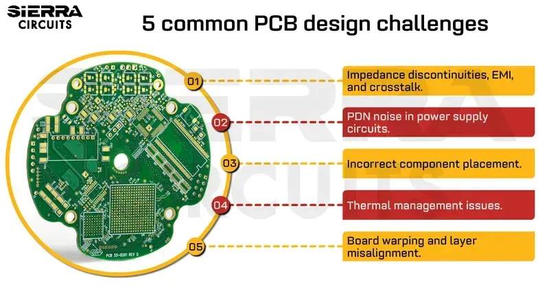
PCB Design Challenges
Designing the Printed Circuit Board (PCB) for portable translators presents a unique set of engineering challenges, primarily driven by the demand for miniaturization, extended battery life, and flawless performance. These devices require a delicate balance between compact form factors, robust signal processing, and efficient power management to ensure accurate, real-time communication. Overcoming these hurdles is paramount for delivering a reliable and high-performing portable translator PCB solution, especially for advanced IoT translator applications where seamless integration and enduring operation are critical.
How does power efficiency impact portable translator PCB design? Power efficiency is central to portable translator design, directly influencing battery life and user experience. The PCB must incorporate advanced power management ICs (PMICs) and optimize component selection for low power consumption, balancing performance with minimal energy draw. This involves careful layout to reduce impedance and heat generation, ensuring the device operates longer on a single charge, a critical factor for user satisfaction in any portable device, including IoT translator solutions.
Challenge
Impact on Portable Translator PCB
Zero One Solution Approach
Miniaturization
Requires multi-layer PCBs, high-density interconnect (HDI) technology, and careful component placement to fit complex circuitry into small enclosures without compromising performance or thermal management.
Utilizes advanced HDI, fine-pitch assembly, and 3D component stacking, leveraging extensive experience in compact PCB design for consumer electronics.
What are the considerations for signal integrity in portable translator PCBs? Maintaining signal integrity is vital for accurate voice capture, processing, and output. High-speed digital and sensitive analog signals can be susceptible to noise and interference. PCB design must employ proper impedance matching, controlled trace routing, grounding strategies, and shielding to prevent signal degradation, ensuring crystal-clear audio and reliable data transfer, which is essential for the accuracy of a voice translator PCB solution.
Challenge
Impact on Portable Translator PCB
Zero One Solution Approach
Signal Integrity
High-frequency audio and data signals demand precise impedance control, minimized crosstalk, and robust grounding to prevent distortion and ensure accurate translation.
Applies advanced routing techniques, impedance matching, and material selection to maintain signal purity across all critical paths.
Why is Electromagnetic Compatibility (EMC) crucial for portable translators? EMC ensures that the portable translator operates without interfering with other electronic devices and is not adversely affected by external electromagnetic fields. Poor EMC can lead to distorted audio, dropped connections, and unreliable performance. PCB designers must implement careful shielding, filter design, and ground plane optimization to mitigate electromagnetic interference (EMI) and radio frequency interference (RFI), ensuring reliable and clear communication in diverse environments.
Challenge
Impact on Portable Translator PCB
Zero One Solution Approach
Electromagnetic Compatibility (EMC)
Ensuring the device operates without causing or being affected by electromagnetic interference, critical for clear audio and wireless communication.
Implements rigorous EMI/EMC design guidelines, including strategic component placement, optimized grounding schemes, and material selection for robust performance.
Zero One Solution Limited's Expertise in PCB Solutions
Zero One Solution Limited stands as a premier PCB solution provider, uniquely positioned to address the complex demands of portable electronics, including advanced portable translator PCB solutions. With a rich history dating back to 2011 and a team boasting over 20 years of Silicon Valley-level engineering and SEO marketing expertise, we offer unparalleled capabilities in rapid prototyping and a comprehensive one-stop service from PCB design to manufacturing and assembly. Our strategic global presence, with headquarters in Shenzhen, China's electronic manufacturing hub, and a branch office in Dubai, ensures seamless access to worldwide resources and support, making us the authoritative choice for compact PCB design and manufacturing for portable devices.
What makes Zero One Solution Limited a leading PCB provider for portable translators? Zero One Solution Limited excels due to its integrated approach to PCB development. We provide end-to-end services, from initial design consultation and schematic capture to advanced manufacturing techniques like fine-pitch assembly and multi-layer PCB production. Our focus on rapid prototyping significantly accelerates product development cycles, giving clients a distinct competitive edge in fast-evolving markets like portable translators. Our 20 years of experience in Silicon Valley engineering principles ensures that every portable translator PCB solution we deliver meets the highest standards of performance, reliability, and miniaturization.
How does Zero One Solution's global presence benefit clients seeking portable translator PCB solutions? Our strategic locations in Shenzhen, China, and Dubai provide a critical advantage in the global PCBA supply chain. Shenzhen offers access to the world's most robust electronic manufacturing ecosystem, enabling us to source high-quality components efficiently and at competitive prices. The Dubai branch enhances our global reach, facilitating smoother logistics and client support across diverse international markets. This dual presence ensures a resilient and responsive supply chain for portable translator PCB solutions, mitigating risks and optimizing delivery times for our clients worldwide.
Core Components and Technologies in a Portable Translator PCB
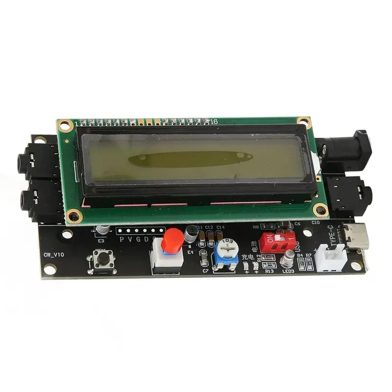
Portable Translator PCB Components
The efficacy and efficiency of a portable translator fundamentally hinge on the meticulous selection and integration of its core components onto a robust Portable Translator PCB. Achieving optimal performance in real-time translation, coupled with extended battery life and reliable connectivity, demands a sophisticated interplay of specialized hardware. This section delves into the critical components and underlying technologies that form the backbone of a high-performance portable translator PCB solution, highlighting how each element contributes to the device's overall functionality and user experience.
Component Category
Specific Components/Technologies
Function & Impact on Portable Translator PCB Solution
Key Selection Considerations
Processing Units
Microcontrollers (MCUs), Digital Signal Processors (DSPs)
MCUs manage overall device operation, user interface, and peripheral control. DSPs are critical for low-latency audio processing, noise reduction, and voice recognition algorithms, directly impacting translation speed and accuracy.
Processing power (MIPS/GHz), power consumption (mW), integrated peripherals (GPIO, SPI, I2C, UART), DSP core capabilities (MAC units, instruction sets), package size for miniaturization.
Memory Modules
SRAM (Static RAM), DRAM (Dynamic RAM), Flash Memory (NOR/NAND)
SRAM provides fast, temporary storage for real-time data. DRAM serves as main system memory for operating system and application data. Flash memory stores firmware, translation models, and user data, enabling offline translation capabilities.
Capacity (MB/GB), speed (MHz), power consumption, read/write endurance for Flash, package type (e.g., LPDDR for low power), cost per bit.
Power Management
Power Management ICs (PMICs), Voltage Regulators, Battery Chargers
Efficiently regulate and distribute power from the battery to all components, ensuring stable operation and maximizing battery life. Critical for miniaturization and thermal management.
Efficiency (%), quiescent current (μA), number of output rails, integration level, protection features (over-voltage, over-current), package size, thermal performance.
Audio codecs convert analog audio signals to digital and vice versa, crucial for clear voice capture and playback. Amplifiers drive speakers. High-quality MEMS microphones ensure accurate speech capture in various environments.
Sampling rate, bit depth, Signal-to-Noise Ratio (SNR), Total Harmonic Distortion (THD+N), power consumption, microphone sensitivity, speaker frequency response, acoustic design integration.
Wireless Connectivity
Wi-Fi Modules (802.11 b/g/n/ac), Bluetooth Modules (BLE/Classic)
Wi-Fi enables high-speed data transfer for online translation services and firmware updates. Bluetooth facilitates connectivity with peripherals like headphones or smartphones, essential for a seamless user experience.
Standards supported, data rates, power consumption (especially for BLE), range, antenna integration options (on-chip, external), security features, coexistence with other wireless technologies.
The strategic selection of these core components, optimized for power, performance, and footprint, is paramount in crafting a superior portable translator PCB solution. Engineers must balance cutting-edge technology with practical considerations to ensure the final product is both highly functional and commercially viable.
Zero One Solution's Tailored Design and Manufacturing Process for Portable Translator PCBs
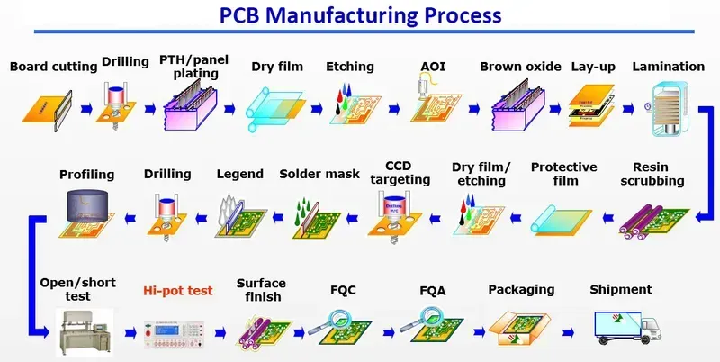
PCB Manufacturing Process
At Zero One Solution Limited, our bespoke design and manufacturing process for Portable Translator PCBs is meticulously crafted to address the unique demands of miniaturization, high performance, and unwavering reliability. Leveraging two decades of Silicon Valley-level engineering expertise, we transform complex requirements into highly efficient and compact PCB solutions, ensuring your portable translator devices not only function flawlessly but also lead the market in innovation and user experience. Our comprehensive approach covers every critical stage, from initial concept to final assembly, with an unwavering focus on precision and quality.
Schematic Capture and Component Selection Our process begins with meticulous schematic capture, translating your functional specifications into an electronic circuit diagram. We strategically select high-performance, energy-efficient components crucial for portable devices, including advanced microcontrollers, compact memory modules, and specialized audio codecs, ensuring optimal performance within stringent power and space constraints. Our engineers meticulously consider every aspect to guarantee a robust foundation for your portable translator PCB.
Advanced PCB Layout for Miniaturization and Signal Integrity Miniaturization is paramount for portable translators. Our experts employ advanced PCB layout techniques, including high-density interconnect (HDI) and multi-layer designs, to achieve the smallest possible footprint without compromising performance. We prioritize signal integrity and power delivery network (PDN) optimization to prevent electromagnetic interference (EMI) and ensure crystal-clear audio processing and reliable wireless communication, which are critical for the portable translator PCB's core functionality.
Strategic Material Selection The choice of PCB materials directly impacts performance and durability. We select advanced substrates (e.g., high-Tg laminates, low-loss materials) that offer superior thermal management, enhanced dielectric properties for high-frequency signals, and mechanical robustness, all essential for the demanding portable environment. This thoughtful material selection extends the lifespan and reliability of your portable translator PCB.
Rapid Prototyping Services Our rapid prototyping capabilities are a cornerstone of our service. We accelerate your product development cycle by quickly producing high-quality prototypes for testing and validation. This iterative process allows for swift design refinements, reducing time-to-market and ensuring the final portable translator PCB meets all functional and performance benchmarks before mass production.
Advanced Manufacturing Techniques Leveraging state-of-the-art manufacturing facilities, we employ advanced techniques such as fine-pitch assembly, ball grid array (BGA) placement, and sophisticated automated optical inspection (AOI). Our controlled manufacturing environment ensures precise component placement and soldering, critical for the compact and complex designs inherent in a portable translator PCB, guaranteeing high yield and consistent quality.
Rigorous Quality Control and Testing Quality is non-negotiable. Our multi-stage quality control process includes comprehensive electrical testing, functional verification, and environmental stress testing. Every portable translator PCB undergoes rigorous inspection to ensure compliance with industry standards and your specific performance requirements, guaranteeing reliability and peak performance in diverse operational conditions.
Benefits of Partnering with Zero One Solution for Portable Translator PCBs
Partnering with Zero One Solution Limited for your portable translator PCB needs offers a distinct competitive edge, transforming development challenges into market opportunities. Our integrated expertise in rapid prototyping, cost-efficient manufacturing, and global supply chain management ensures that your innovative portable translator concepts not only materialize swiftly but also achieve unparalleled performance and reliability. We are committed to being the preferred portable translator PCB provider, driving your success from initial design to mass production.
Accelerated Time-to-Market Our rapid prototyping capabilities dramatically reduce the development cycle. By streamlining PCB design, manufacturing, and assembly into a seamless one-stop service, we enable clients to quickly iterate, test, and launch their portable translator devices, gaining a crucial advantage in fast-paced markets.
Cost-Effective Solutions Without Compromising Quality Leveraging our strategic location in Shenzhen, the global electronics manufacturing hub, and our optimized supply chain, we deliver highly cost-effective portable translator PCB solutions. This efficiency does not come at the expense of quality; our rigorous quality control processes and adherence to industry standards ensure superior product outcomes.
Robust Global Supply Chain Access With a strong presence in Shenzhen and a branch office in Dubai, Zero One Solution Limited operates within a comprehensive global PCBA supply chain network. This ensures reliable access to high-quality components and materials, mitigating supply risks and ensuring consistent production for your portable translator PCB projects.
Expert Engineering Support from Concept to Mass Production Our team of veteran engineers, with two decades of Silicon Valley-level experience, provides unparalleled expert support throughout every phase of your project. From initial concept validation and compact PCB design to complex IoT translator solutions and mass production optimization, our guidance ensures a superior product outcome.
Specialization in Compact PCB Design and IoT Translator Solutions Our deep expertise in compact PCB design is crucial for the miniaturization and high-performance requirements of modern portable translators. Furthermore, our proficiency in IoT translator solutions ensures that your devices are not only compact and efficient but also seamlessly integrate with smart ecosystems, enhancing functionality and user experience.
Zero One Solution Limited's Portable Translator PCB Solution offers a comprehensive, end-to-end service designed to meet the rigorous demands of modern portable devices. From initial concept and design to rapid prototyping, manufacturing, and assembly, our veteran engineers and state-of-the-art facilities ensure your project's success. With our deep industry expertise, global supply chain network, and unwavering commitment to quality, we empower you to deliver cutting-edge, reliable, and compact language translation devices to the market faster than ever before. Don't let PCB complexities slow down your innovation. Partner with Zero One Solution Limited and transform your portable translator vision into reality. Contact us today to discuss your project and discover how our tailored PCB solutions can accelerate your time to market.