
In the world of high-precision test instrumentation, even a microscopic deviation in board architecture can translate into significant signal distortion. When your equipment demands absolute accuracy, standard manufacturing practices simply fall short. This guide bridges the gap between engineering intent and fabrication reality, providing the DFM roadmap necessary to maintain signal integrity and meet the rigorous tolerances required for advanced measurement systems.
The Critical Role of DFM in High-Frequency Test Gear
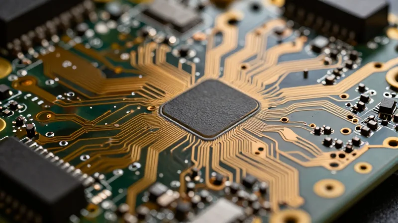
Why Standard PCB Rules Fall Short for High-Frequency Gear
Standard DFM guidelines, typically calibrated for consumer electronics or lower-frequency digital systems, often ignore the parasitic effects that degrade high-frequency signals. In high-precision measurement equipment, trace geometries, dielectric constants, and copper surface roughness act as active components. Failure to treat the PCB as an integrated microwave circuit leads to impedance discontinuities, signal attenuation, and electromagnetic interference that render test results unreliable.
Critical DFM Parameters for Measurement Reliability
| Design Factor | High-Frequency Impact | DFM Optimization Strategy |
|---|---|---|
| Copper Roughness | Increased skin-effect loss | Specify VLP or HVLP copper foils |
| Dielectric Consistency | Phase shift and timing skew | Use materials with low Df/Dk variance |
| Via Geometry | Reflections at high frequencies | Minimize stub length via back-drilling |
Frequently Asked Questions
- How does surface finish affect precision test gear?
Surface finishes like ENIG can impact high-frequency propagation due to the nickel layer's magnetic properties. ENEPIG or Immersion Silver is often preferred for superior signal integrity at microwave frequencies. - Is back-drilling always necessary for high-speed vias?
For frequencies exceeding 5-10 GHz, via stubs act as resonant antennas. Back-drilling is essential to remove these stubs and prevent signal degradation caused by reflections. - Why is the PCB stack-up considered part of DFM?
In high-precision gear, stack-up symmetry is critical to prevent board warp and ensure precise impedance control across differential pairs, which is vital for maintaining common-mode rejection ratios.
Mastering Stack-up Optimization for Impedance Control
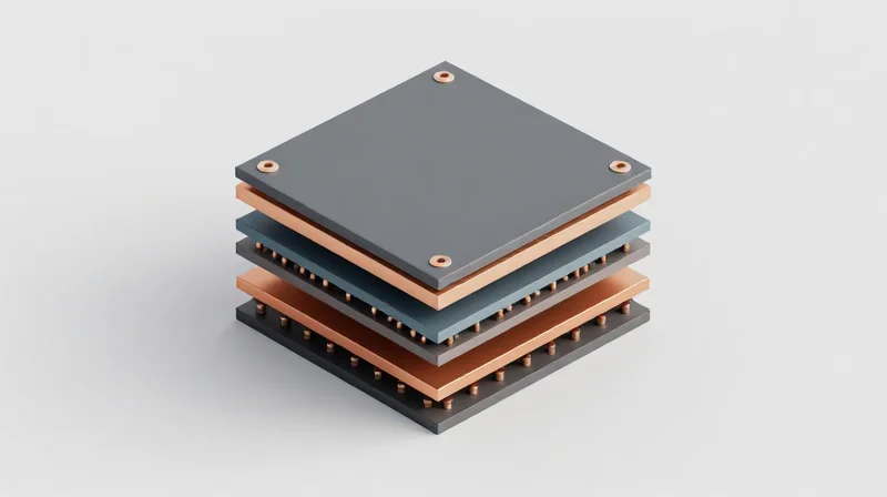
Core Strategies for Impedance-Controlled Stack-ups
Precision measurement equipment demands absolute stability in impedance profiles. To achieve this, engineers must move beyond basic design rules and focus on the physics of the dielectric stack-up. The primary goal is to minimize discontinuities by ensuring that signal propagation remains uniform across every transition, especially in high-speed differential pairs.
Dielectric Selection and Thickness Constraints
Material selection is the first line of defense against signal degradation. Low-loss materials with stable Dielectric Constant (Dk) and Dissipation Factor (Df) across a wide frequency spectrum are essential. When defining thickness constraints, consider the following trade-offs between standard FR-4 and high-performance laminates.
| Material Class | Dk Stability | Insertion Loss | Primary Application |
|---|---|---|---|
| Standard FR-4 | Low | High | General Logic |
| Mid-Loss Laminate | Moderate | Moderate | High-Speed SerDes |
| PTFE/Ceramic-filled | Very High | Very Low | Precision RF/Analog |
Symmetric Planning and Reference Planes
Symmetry in layer stack-up is non-negotiable for high-precision boards to prevent thermal warpage and ensure consistent mechanical impedance. Proper reference plane selection—coupling signal layers to solid ground planes rather than split planes—is critical to maintaining the return path integrity that high-precision measurements require.
- Why is stack-up symmetry important?
Symmetry prevents mechanical stress and warping during the lamination process, ensuring the PCB maintains planarity which is vital for automated test equipment assembly. - What is the role of reference plane coupling?
Tight coupling between the signal trace and a continuous reference plane minimizes return current path length, effectively reducing EMI and parasitic inductance. - How do dielectric tolerances affect precision?
Variations in dielectric thickness directly correlate to impedance fluctuations; specifying 'controlled dielectric' processes from the fabricator is necessary for tight tolerances.
Navigating Trace Geometry and Copper Weight Constraints
Balancing Trace Geometry and Skin Effect
In high-precision measurement hardware, trace geometry is not merely about routing density but managing the electromagnetic field distribution. As signal frequency increases, the skin effect confines current to the outer perimeter of the conductor, making the cross-sectional shape and surface roughness of the copper critical factors. To minimize insertion loss, designers must prioritize wider traces to reduce DC resistance, while maintaining strict spacing rules to mitigate crosstalk and impedance discontinuities.
Copper Weight and Etch Factor Stability
Selecting the appropriate copper weight requires a trade-off between current-carrying capacity and the ability to maintain a consistent etch factor. Heavier copper weights (e.g., 2 oz) are often required for power delivery, but they introduce greater undercutting during the etching process, leading to trapezoidal trace profiles that degrade impedance stability. For precision signals, thinner copper (0.5 oz or 1 oz) is preferred to ensure a near-rectangular cross-section and more predictable transmission line performance.
| Copper Weight | Etch Factor Benefit | Primary Application |
|---|---|---|
| 0.5 oz | Excellent (High Aspect Ratio) | High-Speed Signals/Micro-vias |
| 1.0 oz | Good (Standard Precision) | General Signal Routing |
| 2.0 oz | Limited (Higher Undercutting) | High-Current Power Planes |
DFM Considerations for Trace Geometry
- How does surface roughness affect high-frequency measurements?
As signals move to the outer surface of the copper due to the skin effect, irregularities (roughness) in the foil increase the effective path length and signal attenuation, which can significantly skew sensitive measurement data. - Why is the etch factor critical for impedance control?
The etch factor defines the slope of the trace sidewalls; non-vertical sidewalls alter the capacitance per unit length, making it impossible to achieve target impedance without accounting for manufacturing-specific cross-sectional variations. - What is the rule of thumb for trace spacing in precision gear?
Adhere to the '3W' rule—spacing between traces should be at least three times the trace width—to minimize mutual coupling and maintain EMI isolation in sensitive front-end measurement circuits.
Advanced Fabrication Processes for Tight Tolerances
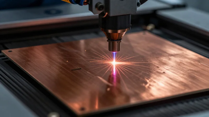
To meet the rigorous demands of complex measurement equipment, standard fabrication limits are insufficient. Advanced processes such as Laser Direct Imaging (LDI) and depth-controlled routing are essential for maintaining the sub-mil alignment necessary for high-density interconnects and sensitive high-speed signal paths.
Key Fabrication Technologies for Precision
| Process | Tolerance Capability | Primary Application |
|---|---|---|
| Laser Direct Imaging (LDI) | +/- 10 microns | Fine-pitch BGA/QFN alignment |
| Controlled Depth Drilling | +/- 25 microns | Back-drilling for stub removal |
| Plasma Desmear | High aspect ratio | Micro-via interconnect integrity |
Ensuring Drill-to-Copper Registration
Registration error is the single greatest risk to high-precision PCB yield. Designers must account for material movement during thermal cycling and lamination. Utilizing oversized capture pads or teardropping is standard, but for ultra-tight tolerances, employing cross-section coupons for real-time registration verification is highly recommended.
- How does LDI improve registration?
LDI eliminates the physical photomask, allowing the system to scale the image dynamically to match actual panel distortion measured during the manufacturing process. - When is sequential lamination required?
Sequential lamination is necessary when the registration requirement exceeds the capability of a single-press cycle, allowing for independent drilling and plating of internal layer sub-assemblies. - What is the impact of etch factor on tolerances?
The etch factor dictates the side-wall profile of copper traces; as width decreases, variation in the etch factor becomes a dominant source of impedance inconsistency.
Minimizing Signal Discontinuities Through Via Design
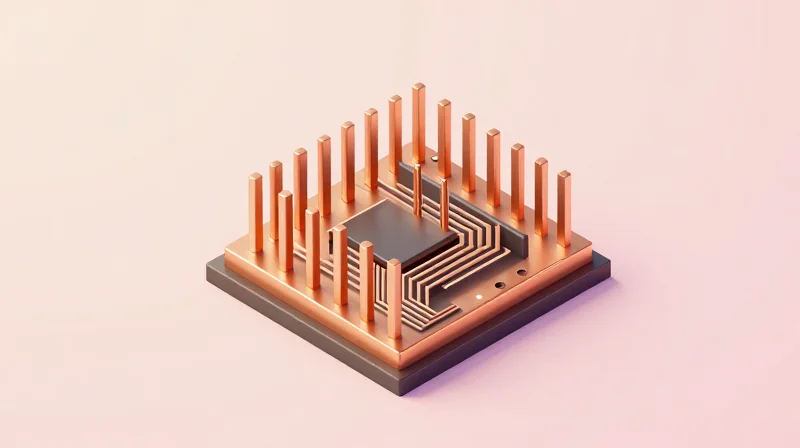
Mitigating Signal Discontinuities in Via Transitions
Vias act as potential points of signal reflection and resonance in high-speed circuits due to the impedance mismatch between the transmission line and the vertical barrel. To minimize discontinuities, engineers must focus on reducing parasitic capacitance and optimizing the transition geometry.
Strategic Via Management Techniques
- Back-Drilling Stub Removal
Removing unused via stubs via controlled-depth drilling prevents signal reflections at high frequencies, which otherwise act as antennas and cause significant resonance. - Via-in-Pad with Conductive Fill
Utilizing via-in-pad (VIPPO) allows for shorter escape routes, reducing inductance, provided the vias are plugged and plated over to ensure planarity and thermal conductivity. - Optimizing Anti-Pad Dimensions
The clearance hole in the reference plane (anti-pad) must be carefully sized; too small increases parasitic capacitance, while too large can lead to return path discontinuities.
| Via Technique | Best Used For | Key DFM Constraint |
|---|---|---|
| Back-Drilling | High-speed data lines | Requires strict drill-to-layer depth tolerance |
| VIPPO | Fine-pitch BGA routing | Requires conductive epoxy fill and plating |
| Stitching Vias | Ground return path stability | Must be placed symmetrically to avoid skew |
To achieve high-precision results, always maintain a stitching via near every signal layer transition. This provides a clear return path and minimizes the loop area, effectively reducing electromagnetic interference (EMI) risks.
Surface Finish Impacts on High-Frequency Performance
The Physics of Surface Finish and Signal Integrity
At high frequencies, the skin effect confines the electromagnetic current to the outer layer of the conductor. As signal speeds increase, the surface finish—once considered a minor assembly detail—becomes a primary contributor to insertion loss. Variations in conductivity, surface morphology, and thickness of the plating layers directly influence return loss and signal attenuation, necessitating precise selection based on the specific frequency requirements of the instrument.
| Finish Type | Conductivity | High-Freq Suitability | Primary Limitation |
|---|---|---|---|
| ENIG | Moderate | Good | Nickel resonance/Loss |
| ENEPIG | Moderate | Excellent | Complex process control |
| Immersion Silver | High | Excellent | Susceptibility to tarnish |
Evaluating Finishes for High-Precision Applications
- Does ENIG cause signal degradation?
ENIG can introduce losses due to the presence of the nickel layer. Because nickel is ferromagnetic and possesses higher resistivity than copper, the skin effect penetration into the nickel layer at high frequencies can increase resistive losses and degrade signal integrity. - Why is ENEPIG preferred for RF designs?
ENEPIG (Electroless Nickel Electroless Palladium Immersion Gold) provides a thin palladium barrier that prevents the migration of nickel into the gold layer and offers a more uniform surface, reducing insertion loss compared to traditional ENIG. - Is Immersion Silver superior for high-speed transmission?
Immersion Silver offers the highest conductivity among common finishes and is extremely flat, which is beneficial for fine-pitch high-frequency traces. However, it requires careful storage to avoid oxidation and sulfur contamination, which can impact performance over time.
For design engineers, the selection process must prioritize the surface profile. Excessive roughness—whether from the copper foil or the applied finish—leads to increased effective path length and higher dielectric absorption. To maximize performance in high-precision measurement systems, designers should opt for finishes that provide the lowest possible skin depth interference while ensuring long-term solderability and environmental stability.
Effective Collaboration with PCB Fabricators
Bridging the Design-to-Fabrication Gap
Effective collaboration relies on proactively sharing your design intent and acknowledging the physical limitations of your fabricator’s specialized equipment. Rather than waiting for a DFM review to flag issues, integrating your manufacturing partner into the early stages of the layout ensures that critical features like controlled impedance profiles and registration tolerances are achievable with their specific stack-up and processing capabilities.
Key Communication Strategies
- Define Critical-to-Function (CTF) Features
Explicitly label features requiring the tightest tolerances, such as high-speed signal paths, impedance-controlled traces, and precision registration points, so the manufacturer can prioritize these during processing. - Share Stack-up Specifications Early
Provide detailed material properties, layer sequencing, and copper weight requirements before finalizing the board layout to avoid post-layout impedance mismatches. - Align on Fabrication Tooling Constraints
Discuss drill sizes, via aspect ratios, and minimum annular ring requirements to ensure your design does not exceed the manufacturer’s reliable production limits.
Comparison of Documentation Quality
| Documentation Feature | Reactive Approach (Suboptimal) | Proactive Approach (Best Practice) |
|---|---|---|
| Material Selection | Generic FR-4 designation | Specific Tg, Dk, and Df values provided |
| Impedance Data | Single target value | Target value + allowable variance + stack-up |
| Tolerance Notes | Standard industry specs | Custom requirements for specific critical layers |
Finally, utilize formal DFM feedback loops to refine your design libraries. Treat every flagged tolerance violation not merely as a hurdle, but as data to calibrate your future layout decisions, ultimately creating a more robust design-for-manufacturability cycle.
Achieving precision in test equipment requires a seamless integration of design intent and manufacturing capability. By applying these DFM strategies, you can minimize board-level variances and ensure the repeatable accuracy your instruments demand. Ready to refine your next design? Contact our engineering team today for a technical review of your high-frequency PCB requirements.
