
In the fast-paced world of industrial automation, the bottleneck is often the hardware. As machine vision systems demand higher speeds and smaller footprints, engineers face significant DFM hurdles. This article provides a masterclass in designing robust HDI PCBs that survive the noise and heat of factory environments.
Understanding the HDI Challenge in Machine Vision

The Shift from Standard PCB to HDI in Machine Vision
Next-generation industrial machine vision systems demand ultra-compact footprints to accommodate high-resolution sensors and high-speed processing units. Traditional PCB design rules rely on larger via geometries and wider trace spacing, which inherently fail to support the high-density interconnect (HDI) requirements of these sophisticated modules. As signal speeds climb into the multi-gigabit range, the legacy approach to layer stack-ups and routing leads to catastrophic signal attenuation, excessive crosstalk, and thermal bottlenecking that compromises image capture accuracy.
Comparison of Traditional vs. HDI Design Constraints
| Feature | Traditional PCB | HDI PCB |
|---|---|---|
| Via Structure | Through-hole | Microvia (Blind/Buried) |
| Component Pitch | > 0.8mm | < 0.5mm |
| Trace/Space | 5+ mil | 2-3 mil |
| Signal Integrity | Limited at High Speed | Optimized for High Speed |
Why Traditional DFM Fails
- Signal Integrity (SI) Degradation
Traditional through-hole vias create long stubs that act as parasitic radiators, causing reflections and resonance in high-speed differential pairs, which is unacceptable for high-bandwidth CMOS sensor interfaces. - Thermal Management Limitations
Standard routing lacks the sophisticated heat dissipation pathways needed for high-performance SoCs and FPGAs, often leading to thermal throttling that degrades machine vision reliability in industrial environments. - Interconnect Density Constraints
Legacy rule sets cannot support the dense BGA pinouts of modern processors, leading to breakout failure or the need for excessive, expensive layer counts.
Advanced Stack-up Optimization Strategies
Balancing Layer Count and Signal Integrity
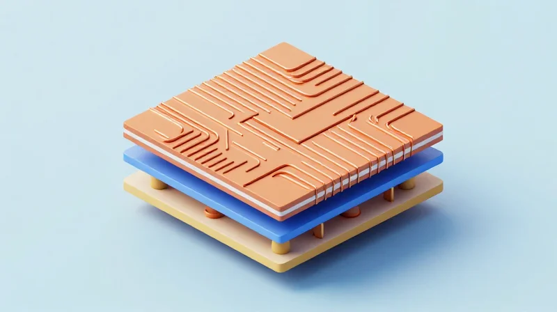
For industrial machine vision systems, the primary goal is minimizing layer count without compromising the impedance environment of high-speed differential pairs like MIPI CSI-2 or GMSL interfaces. Designers must transition from standard sequential lamination to Any-Layer HDI (ELIC) architectures to reduce via stub interference while maintaining a clean reference plane geometry.
| Strategy | Primary Benefit | Design Trade-off |
|---|---|---|
| ELIC Technology | Improved signal routing density | Higher fabrication costs |
| Symmetric Stack-up | Minimized board warpage | Increased layer count |
| Back-drilling | Reduced parasitic resonance | Increased manufacturing complexity |
Advanced Thermal Dissipation Tactics
Machine vision sensors generate significant localized heat. Advanced stack-up optimization utilizes integrated copper coins or high-thermal-conductivity prepregs directly under the image sensor package. By coupling thermal vias directly to internal ground planes, you create a low-impedance thermal path that prevents color noise and frame rate degradation.
Critical Optimization FAQ
- How does stack-up affect EMI in machine vision?
A well-optimized stack-up maintains tight coupling between signal layers and their adjacent reference planes, effectively containing electromagnetic fields and reducing radiated emissions in compact enclosures. - Should I prioritize layer count or signal integrity?
In high-speed imaging applications, signal integrity must always take precedence; an optimized stack-up should use thinner dielectrics to maintain impedance, even if it forces a slightly higher layer count. - Is buried via usage recommended?
Yes, buried vias are essential for escaping high-pin-count BGA sensors, as they free up surface routing space and reduce parasitic capacitance associated with through-hole stubs.
Micro-via Technology and Aspect Ratio Best Practices
Micro-via Design and Aspect Ratio Limits
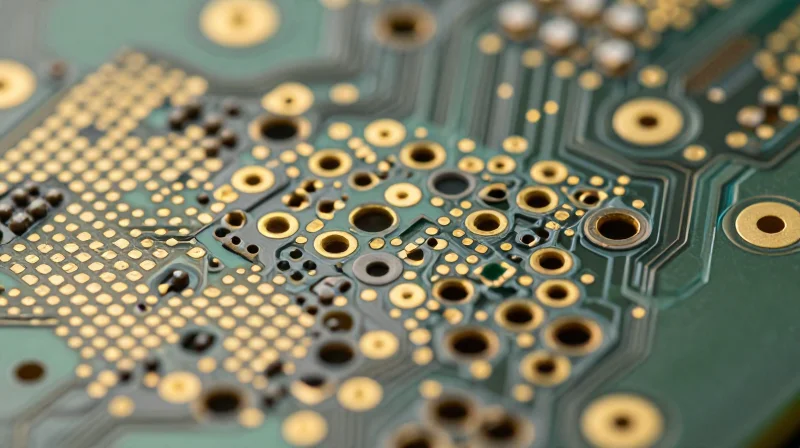
In industrial machine vision systems, where high-speed signal integrity and miniaturization are paramount, micro-via reliability is the critical failure point. To ensure robust interconnections, the aspect ratio (depth-to-diameter) of laser-drilled micro-vias must be kept below 0.75:1. Exceeding this limit often results in incomplete plating, creating void spaces that lead to thermal stress fractures during operation.
| Via Type | Recommended Aspect Ratio | Primary Application |
|---|---|---|
| Micro-via (Laser) | 0.75:1 or less | High-density signal routing |
| Stacked Via | 1:1 (Max) | High-speed layer transitions |
| Through-hole (Mechanical) | 10:1 | Power and Ground distribution |
Best Practices for Plating and Reliability
- How does via-in-pad affect assembly?
Using via-in-pad, particularly with copper-filled micro-vias, eliminates the risk of solder wicking into the via barrel, which is essential for stable BGA mounting in compact vision modules. - Why is copper-capping mandatory?
Plated-over filled vias (via-in-pad) must be planarized and capped with copper to prevent surface indentations that compromise solder joint integrity during reflow. - Can I use stacked vias for better routing?
Stacking is acceptable but requires high-precision alignment and filled structures; otherwise, staggered vias are preferred to reduce the structural stress concentration on the laminate.
Drafting Rules for Laser Drilling
For HDI designs targeting sub-millimeter pitches, ensure that the annular ring requirements meet IPC-2226 Class 3 standards. Laser energy must be carefully calibrated to the specific dielectric material to avoid 'nail-heading' or excessive resin recession, both of which can compromise the long-term reliability of machine vision modules operating in harsh, high-vibration industrial environments.
Signal Integrity and Routing in Dense Environments
Strategies for Signal Integrity in Dense Layouts
In high-density interconnect (HDI) PCBs for machine vision, signal integrity (SI) is compromised by increased trace density, closer proximity of high-speed differential pairs, and reduced distance to the reference plane. To maintain signal fidelity, designers must move beyond standard clearance rules and implement rigorous crosstalk suppression techniques. Priority should be placed on maintaining consistent reference planes and utilizing length matching that accounts for the dielectric variation inherent in multi-layer HDI structures.
Mitigating Electromagnetic Interference (EMI)
Industrial vision modules operate in electrically noisy environments. EMI mitigation requires a multi-layered approach centered on return path management and stack-up symmetry.
| EMI Mitigation Strategy | Implementation Detail | Primary Benefit |
|---|---|---|
| Stitching Vias | Add ground vias near signal transitions | Reduces loop inductance |
| Differential Impedance | Tight coupling of pairs to ground planes | Minimizes common-mode noise |
| Plane Segregation | Isolate analog and digital power zones | Prevents supply ripple crosstalk |
Routing Best Practices FAQ
- How do I calculate trace spacing in extremely dense areas?
Utilize the 3W rule (separation equal to three times the trace width) as a baseline, but validate with field solvers to account for the impact of thin-core laminates common in HDI. - Is back-drilling necessary for high-speed machine vision signals?
Yes. For data rates exceeding 5Gbps, stub lengths on vias act as resonant antennas; back-drilling is essential to remove these stubs and maintain channel integrity. - How does HDI stack-up affect EMI shielding?
Using a balanced build with internal ground planes serving as shields for sensitive signal layers effectively traps return currents and isolates noisy high-speed buses.
Managing Thermal Dynamics in Enclosed Systems

Thermal Dynamics in Enclosed Vision Systems
In next-generation industrial machine vision systems, the shift toward compact enclosures creates a significant thermal management bottleneck. High-density interconnect (HDI) PCBs, characterized by dense component population and high-speed processing, generate localized heat flux that can lead to thermal throttling and signal degradation. Design for Manufacturing (DFM) must prioritize heat spreading across internal layers to prevent reliability failures within hermetically sealed or fanless environments.
Strategies for Heat Dissipation
- Thermal Via Arrays
Utilize high-density micro-via arrays directly beneath high-TDP processors to conduct heat into internal ground planes, serving as integrated heat spreaders. - Copper Weight Optimization
Increase copper thickness on internal layers dedicated to heat distribution, balancing this against the impedance requirements of high-speed routing. - Component Partitioning
Isolate high-heat generation components from temperature-sensitive sensors and high-speed signal pathways to minimize thermal cross-coupling.
| Thermal Strategy | Effectiveness | Manufacturing Complexity |
|---|---|---|
| Thermal Vias | High | Moderate |
| Thick Copper Planes | High | Low |
| Component Partitioning | Moderate | High |
| Heat Pipes/Sinks | Very High | Very High |
FAQ: Managing Heat in Dense Enclosures
- How does HDI influence thermal design?
HDI structures allow for denser routing, but the reduced PCB volume limits the material available to absorb and distribute heat, necessitating active use of copper planes. - Can thermal vias impact signal integrity?
Yes, excessive via stubs can cause signal reflections; therefore, thermal vias must be carefully placed to avoid interrupting critical high-speed return paths.
Surface Finish and Solder Mask Selection for Reliability
In next-generation machine vision systems, where PCBs are often subjected to mechanical vibration, thermal cycling, and harsh industrial pollutants, the interface between components and the board substrate must be uncompromisingly stable. Surface finish selection dictates the oxidation resistance and soldering integrity, while the solder mask must provide superior adhesion and thermal expansion compatibility to prevent delamination.
Surface Finish Comparative Analysis
| Finish | Solderability | Flatness | Industrial Suitability |
|---|---|---|---|
| ENIG | Excellent | Superior | High: Good for fine pitch/BGA |
| ENEPIG | Excellent | Superior | Very High: Robust for multi-cycle/wire bond |
| Immersion Silver | Good | High | Moderate: Prone to tarnishing |
| HASL (Lead-Free) | Excellent | Poor | Low: Not ideal for HDI high-density |
Optimizing Solder Mask Performance
For HDI designs with ultra-fine pitch components, standard liquid photo-imageable (LPI) solder masks may suffer from registration issues or lack of resolution. Utilizing high-resolution LPI masks or alternative dry-film resists is essential. Furthermore, specifying a low-CTE (Coefficient of Thermal Expansion) mask material helps mitigate the risk of micro-crack formation at the solder joint interface during the frequent thermal transitions inherent in high-performance imaging sensors.
Reliability FAQ
- Why is ENEPIG preferred over ENIG for high-reliability industrial vision systems?
ENEPIG (Electroless Nickel Electroless Palladium Immersion Gold) eliminates the 'black pad' risk associated with ENIG and provides superior mechanical strength and oxidation resistance, making it ideal for systems requiring extended operational life. - How does solder mask dam spacing affect HDI reliability?
Insufficient dam width between pads can lead to solder bridging during reflow. For HDI boards, maintaining a minimum dam width of 75-100 microns is critical to ensure electrical isolation and prevent ionic contamination buildup. - Does the solder mask color impact thermal dissipation?
While dark colors like matte black are often chosen for optical cleanliness in machine vision, they can slightly alter emissivity. For thermally intensive boards, white or standard green masks are generally preferred for optimal heat dissipation properties.
Design for Assembly (DFA): Ensuring Manufacturability

Optimizing Component Placement for Automated Assembly
In HDI systems, component density is high, but assembly reliability depends on the spatial logic of the PCB layout. To ensure manufacturability, designers must account for pick-and-place precision, solder stencil aperture clearance, and the prevention of thermal shadowing during reflow. Placing components with consistent orientation and maintaining adequate keep-out zones around fine-pitch BGAs and micro-passives is non-negotiable for high-speed industrial assembly.
Standardizing Assembly Parameters
| Feature | Design Constraint | DFA Benefit |
|---|---|---|
| Component Spacing | Minimum 10-15 mil gap | Prevents solder bridging/shorts |
| Fiducial Marks | Minimum 3, corner placement | Ensures precise board alignment |
| Panelization | V-score or tab-routing | Reduces handling stress on PCB |
Frequently Asked Questions regarding HDI Assembly
- How does component orientation impact yield?
Uniform orientation of components reduces the number of rotation steps required by the pick-and-place machine, effectively reducing cycle times and lowering the probability of placement errors. - Why is board panelization critical for vision systems?
Proper panelization maintains board rigidity during assembly, preventing warping that leads to misaligned solder deposits and unreliable electrical connectivity in delicate high-density traces. - What is the primary risk of neglecting DFA in HDI?
The primary risk is a significantly lower First Pass Yield (FPY) caused by solder bridging at fine pitches and component tombstoning due to improper thermal profiles or restrictive keep-out areas.
Standardizing Quality Assurance for High-Speed Designs
Defining Inspection Metrics for High-Density Interconnects
High-density interconnects introduce unique failure modes, including micro-via fatigue and inner-layer registration misalignment, which cannot be captured by standard AOI alone. Standardizing quality assurance requires a multi-tier inspection strategy that prioritizes non-destructive analysis and structural verification during the prototyping phase.
| Inspection Metric | Target Technology | Purpose |
|---|---|---|
| Registration Accuracy | Laser Drilled Micro-vias | Preventing open circuits in high-layer count builds |
| Copper Plating Uniformity | Through-hole Barrels | Ensuring reliability under thermal cycling |
| Solder Void Percentage | BGA/LGA Interconnects | Mitigating intermittent signal loss in vision sensors |
Essential Testing Protocols for Prototype Validation
- Why is Automated X-Ray Inspection (AXI) mandatory for HDI?
AXI is essential for detecting hidden defects in multi-level micro-via structures and BGA solder joints that standard optical systems cannot penetrate. - What role does Cross-Sectional Analysis play in DFM?
Cross-sectional analysis provides destructive proof of laminate integrity and plating thickness, validating that the manufacturing process meets strict structural design requirements. - How does Thermal Shock Testing impact reliability?
Industrial machine vision systems often operate in fluctuating temperatures; cycling prototypes ensures the via-in-pad transitions and material interfaces can withstand expansion without cracking.
Streamlining Verification via Digital Twins
To reduce time-to-market for complex industrial vision systems, design teams should integrate DFM feedback loops with manufacturing digital twins. By correlating real-world inspection data with theoretical simulation models, engineers can refine PCB layouts in subsequent iterations to eliminate persistent manufacturing defects, ultimately enhancing yield rates for high-density, complex boards.
Mastering DFM is the difference between a failing prototype and a production-ready vision system. By adhering to these strict design parameters, you ensure your industrial applications remain reliable and efficient at scale. Contact our engineering team today to review your current PCB stack-up and design files for manufacturability.
