Exploring the PCBWay Factory: A Deep Dive into PCB Manufacturing
2025.01.07
In today's tech-driven world, printed circuit boards (PCBs) are the unsung heroes powering countless devices. The PCBWay factory stands at the forefront of PCB manufacturing, employing cutting-edge technology to produce high-quality boards. This article explores the inner workings of the PCBWay factory, shedding light on the processes, technologies, and capabilities that make them a leading PCB manufacturer.
PCBWay Factory Overview: Location and Scale
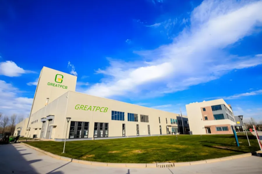
PCB Factory Exterior
The PCBWay factory is strategically located in Shenzhen, China, a global hub for electronics manufacturing. This location provides a significant advantage, allowing PCBWay to efficiently serve a worldwide clientele with rapid prototyping and mass production capabilities. Understanding the physical scale and location of the facility is crucial for assessing their capacity to handle diverse project requirements and global distribution.
Aspect
Details
Location
Shenzhen, China
Strategic Advantage
Access to robust supply chain, skilled labor and advanced tech ecosystem
Global Reach
Serves customers across various continents
Production Capacity
Capable of both prototype and mass production
PCB Prototyping and Manufacturing Processes
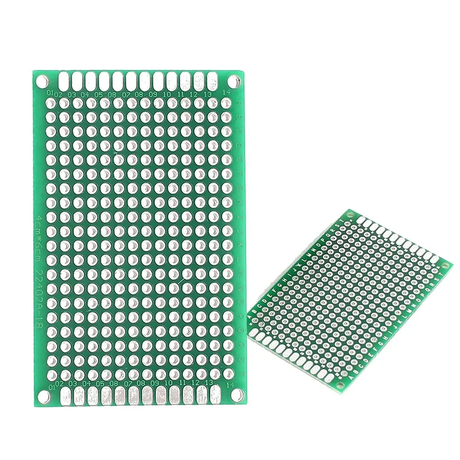
PCB Prototype
The PCBWay factory employs a rigorous and multifaceted approach to PCB manufacturing, transforming initial design concepts into tangible circuit boards. The process encompasses a series of intricate steps, from design verification to final product inspection, each playing a crucial role in ensuring the quality and functionality of the finished product. Key stages include design review, material preparation, etching, drilling, lamination, and surface finishing, followed by meticulous quality control.
The PCB manufacturing process at PCBWay is a detailed sequence of steps designed to accurately reproduce the designed circuit layout onto a physical substrate. Below is a breakdown of the major stages involved:
Design Verification The process begins with a thorough review of the customer's design files. This includes checking for design rule compliance, ensuring all specified parameters are achievable, and verifying the circuit layout for errors.
Material Preparation High-quality base materials, typically fiberglass (FR-4), are selected and cut to the appropriate sizes. The chosen material will affect the final product performance, including thermal and electrical properties. Other materials may be used based on custom requirements.
Layer Imaging Using a photographic process, the circuit pattern is transferred onto the copper layers of the PCB material. The board is coated with a photosensitive film and then exposed to ultraviolet light through a photomask which contains the circuit patterns. The unexposed material is then developed away leaving behind the desired pattern.
Etching The exposed copper that is not protected by the developed photoresist is chemically removed, leaving only the desired copper tracks and pads. This is a critical process that ensures the accuracy of the circuits.
Drilling Precision drilling machines create holes for component leads and vias. The hole size and position are critical for proper assembly and function of the PCB. Drill sizes may range from 0.1mm to several millimeters, depending on the design.
Lamination For multi-layer PCBs, layers of copper circuitry are stacked and laminated together under high heat and pressure, bonding the layers into a single structure using resin. This process is critical for the structural integrity of the final product.
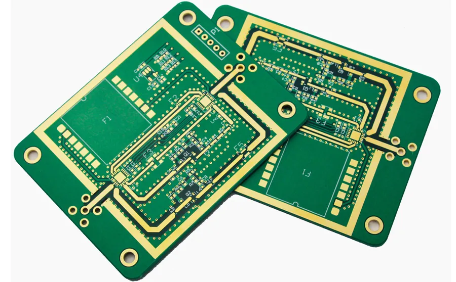
Solder Mask Application A solder mask is applied to the outer layers of the PCB to prevent solder from bridging between traces and pads during assembly. This coating typically provides a green protective layer, which can be customized in different colors.
Surface Finishing The PCB is finished with a coating such as HASL (Hot Air Solder Leveling), ENIG (Electroless Nickel Immersion Gold), or other surface treatments to improve solderability and prevent oxidation of the exposed copper.
Quality Inspection Each finished board undergoes a final automated optical inspection (AOI) and electrical testing to ensure proper fabrication. This final verification stage helps identify any defects prior to shipment.
Advanced Equipment and Technology at PCBWay
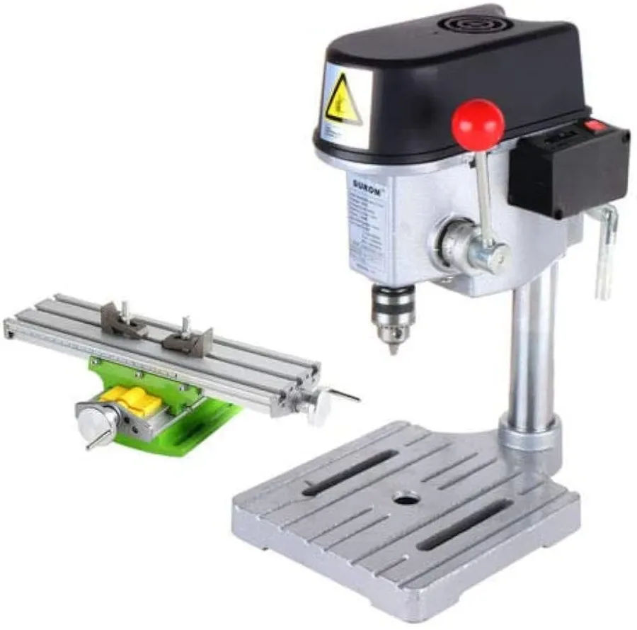
PCB Drilling Machine
PCBWay leverages a suite of advanced manufacturing equipment and technologies within its facility to ensure high-precision and quality in PCB fabrication. This investment in state-of-the-art machinery is crucial for meeting the stringent demands of modern electronics manufacturing, enabling PCBWay to produce complex and reliable circuit boards.
The advanced equipment and technology in PCBWay's factory include:
Automated Optical Inspection (AOI) AOI systems utilize high-resolution cameras and image processing algorithms to automatically inspect PCBs for defects, such as shorts, opens, and incorrect component placement. This technology is crucial for catching errors early in the production process and maintaining consistent quality.
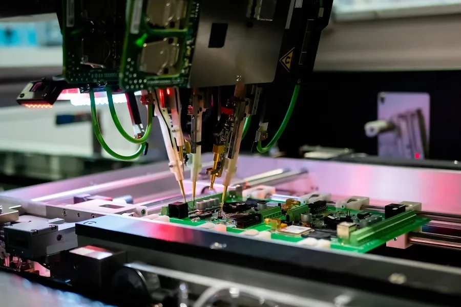
Flying Probe Testing Flying probe testers use movable probes to electrically test PCBs. This is particularly useful for prototype and low-volume production as it avoids the need for custom test fixtures. It allows for a quick and flexible electrical verification of circuit connectivity and performance.
Surface Mount Technology (SMT) Equipment SMT lines consist of pick-and-place machines, solder paste printers, and reflow ovens. These automated machines enable the high-speed and accurate placement of surface mount components, which are typically very small. This leads to higher component density and more compact designs. The reflow ovens ensure precise solder joint formation, leading to more reliable and better performance of electronic devices.
Drilling and Routing Machines These CNC machines are critical for the precise creation of vias, mounting holes, and the final shape of the PCBs. High-precision drilling is essential for multilayer boards that require connection of circuits through multiple layers.
Lamination Equipment Lamination presses are used to bond the various layers of a multilayer PCB together using heat and pressure. Controlled heat and pressure ensures high-integrity PCB construction and reliability of the layers.
Etching Equipment This equipment uses chemical processes to remove copper from the PCB, leaving behind the desired circuit pattern. Precision in this step is critical for the final functionality of the PCB.
The integration of these advanced technologies at PCBWay directly translates into enhanced quality, improved precision, and faster turnaround times, reinforcing their capacity to meet diverse customer needs across a range of industries.
PCB Assembly Services: SMT and Beyond
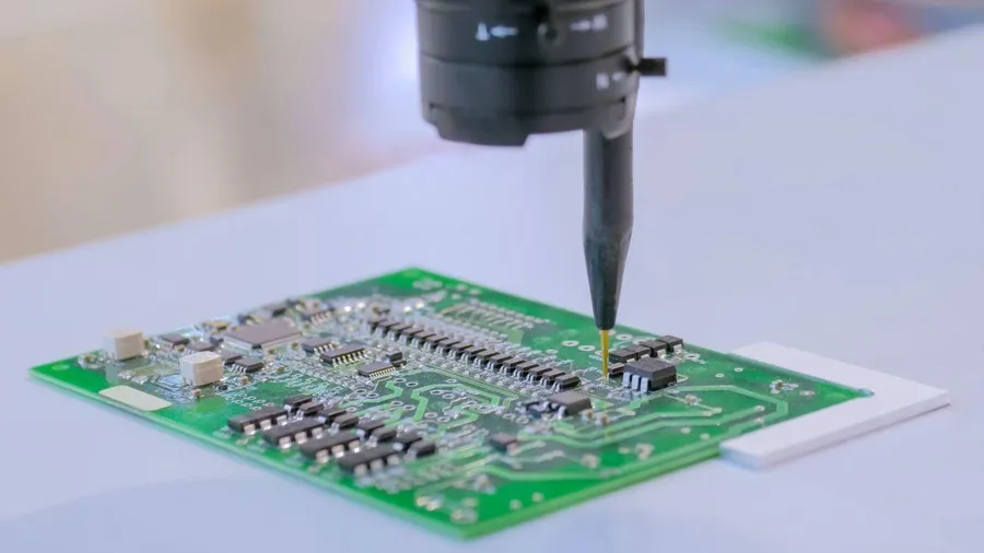
SMT Assembled PCB
PCBWay provides comprehensive PCB assembly services, encompassing Surface Mount Technology (SMT), through-hole assembly, and a variety of related processes. Their capabilities cater to a broad spectrum of production needs, from rapid prototyping to low-to-mid volume manufacturing runs, ensuring they meet diverse client requirements.
The SMT process involves the precise placement of components onto the surface of the PCB using automated machinery, followed by reflow soldering to create permanent electrical connections. Through-hole assembly, on the other hand, is utilized for components that require leads to be inserted through holes in the board and then soldered on the opposite side. Both methods are essential for different types of electronic designs.
Assembly Service
Description
Typical Application
Surface Mount Technology (SMT)
Automated placement of components on the PCB surface, followed by reflow soldering.
High-density boards, small components, automated assembly
Through-Hole Assembly
Insertion of components with leads through holes in the PCB, followed by wave or selective soldering.
Larger components, manual assembly, more robust connections
Mixed Assembly
Combines SMT and Through-Hole Assembly techniques on the same board.
Complex boards with a variety of components
Prototype Assembly
Assembly services tailored for small quantities to test and validate designs.
Design validation, proof-of-concept
Low-to-Mid Volume Assembly
Assembly services for small to medium sized production runs.
Small batch production, iterative design
PCBWay's assembly services leverage a combination of advanced robotics and skilled technicians to ensure both accuracy and efficiency. They offer a range of supplementary services, including component procurement, stencil fabrication, and post-assembly testing, streamlining the overall manufacturing process for their clients.
Quality Control Measures at PCBWay
PCB Testing Equipment
PCBWay employs rigorous quality control measures throughout the entire PCB manufacturing process to ensure high standards of reliability and performance. This commitment to quality is paramount in delivering PCBs that meet or exceed customer expectations and industry standards. Their multi-faceted approach to quality assurance includes stringent testing, inspection protocols, and adherence to international quality certifications.
Design Review and Verification Prior to production, PCBWay conducts thorough design reviews to identify potential manufacturability issues. This early-stage verification is crucial for preventing errors and ensuring the design aligns with fabrication capabilities.
Automated Optical Inspection (AOI) AOI is employed to visually inspect PCBs at various stages of manufacturing. This technology identifies defects, such as shorts, opens, and incorrect component placement with high precision, ensuring consistency and quality throughout the production run.
Electrical Testing PCBWay utilizes electrical testing methods, including flying probe and bed-of-nails testing, to verify the connectivity and functionality of each circuit board. These tests are vital for identifying any electrical faults before the boards are shipped to customers.
Dimensional Accuracy Checks Precise measurements and dimensional checks are performed to ensure that each PCB conforms to the specified dimensions and tolerances. This guarantees proper fit and function within the intended applications.
Final Visual Inspection A final visual inspection by trained personnel is conducted to identify any cosmetic defects or inconsistencies that might have been missed during the automated checks. This ensures that only flawless PCBs are released to the market.
Quality Certifications and Standards PCBWay adheres to international quality certifications, such as ISO 9001, which provides a framework for implementing and maintaining a robust quality management system, ensuring consistency, reliability, and continuous improvement in the manufacturing process.
PCBWay's Customization Capabilities
Custom PCBs
PCBWay distinguishes itself by offering extensive customization options for PCB manufacturing and assembly, catering to diverse client needs. This adaptability is crucial for projects with specific requirements beyond standard specifications.
Material Selection PCBWay provides a variety of materials beyond standard FR-4, including high-frequency laminates (e.g., Rogers, Teflon) for specialized applications, aluminum substrates for better thermal management, and flexible materials for non-rigid designs. This enables engineers to select materials that best fit their electrical, thermal, and mechanical requirements.
Layer Count Flexibility From single-layer boards for basic applications to complex multi-layer boards with up to 32 layers, PCBWay's manufacturing capabilities can accommodate a wide range of design complexities. This flexibility is essential for projects that require high component density and sophisticated signal routing.
Custom Finishes and Solder Masks Options include various surface finishes (e.g., ENIG, HASL, OSP), solder mask colors (beyond the standard green), and specialized finishes for enhanced corrosion resistance or solderability. These options are not merely aesthetic; they can impact the reliability and performance of the final product.
Special Requirements Handling PCBWay accommodates special requests like controlled impedance designs, blind and buried vias, via-in-pad technology, and other advanced features that are crucial for high-speed or high-density designs. Their ability to handle these specialized design elements sets them apart from standard PCB manufacturers.
Advanced PCB Features Capabilities include custom board shapes, specific copper weights, and specialized silkscreen options, allowing for complete design control. These are essential for applications where dimensional constraints, heat dissipation, or labeling are paramount.
Signal Integrity, Miniaturization, High-Density Interconnect
Other
Custom Shapes, Copper Weight, Silkscreen Options
Form Factor, Heat Dissipation, Assembly and Identification
Frequently Asked Questions About PCBWay Factory
This section addresses frequently asked questions regarding the PCBWay factory, including its operational locations, shipping origins, manufacturing capabilities, and comparisons with other PCB manufacturers like JLCPCB. These answers aim to provide clear and concise information to help users understand PCBWay's operations and offerings.
Where is PCBWay's manufacturing facility located? PCBWay's primary manufacturing facility is located in Shenzhen, China, a major hub for electronics manufacturing. This location allows them to leverage a robust supply chain and skilled workforce, ensuring efficient and cost-effective PCB production.
From where does PCBWay ship its products? PCBWay ships its products directly from its manufacturing facility in Shenzhen, China. Depending on the destination, they utilize various shipping methods to ensure timely and reliable delivery to customers worldwide.
What types of PCB manufacturing services does PCBWay offer? PCBWay provides a comprehensive range of PCB manufacturing services, including prototyping, small to large-scale production runs, single-sided, double-sided, and multi-layer PCBs, as well as specialized options like flex PCBs, metal core PCBs, and high-frequency PCBs. They also offer PCB assembly services.
Does PCBWay offer PCB assembly services? Yes, PCBWay offers comprehensive PCB assembly services, including surface mount technology (SMT) assembly, through-hole assembly, and mixed assembly options. They can handle both prototype and production quantities, providing a complete solution from PCB fabrication to finished assembly.
How does PCBWay compare to JLCPCB in terms of service and quality? Both PCBWay and JLCPCB are reputable PCB manufacturers. PCBWay is often preferred for its more extensive service options and ability to handle more complex boards, while JLCPCB is known for its lower prices on standard PCBs. The choice depends on specific project requirements and budget considerations. (See the 'Comparing PCBWay with Other PCB Manufacturers' section for a detailed comparison)
What is the typical lead time for PCB production at PCBWay? The lead time at PCBWay varies based on the complexity of the PCB and the quantity required. Simple prototypes can often be produced within a few days, while more complex or higher-volume orders may take one to two weeks, depending on the fabrication and assembly requirements. Delivery time is separate and depends on the shipping method chosen.
Does PCBWay provide any testing and quality assurance during the manufacturing process? Yes, PCBWay implements rigorous quality control measures throughout the manufacturing process. They use automated optical inspection (AOI), flying probe testing, and other quality testing methods to ensure the PCBs meet high-quality standards and customer specifications. They also follow industry standard certifications.
Comparing PCBWay with Other PCB Manufacturers
A thorough comparison between PCBWay and other PCB manufacturers, most notably JLCPCB, is essential for informed decision-making when selecting a fabrication partner. This analysis delves into critical aspects such as pricing structures, lead times, manufacturing capabilities, and customer feedback to present a comprehensive overview.
Feature
PCBWay
JLCPCB
Pricing
Variable; often competitive for prototypes and small batches; tiered pricing for larger quantities
Generally lower for basic prototypes and small to medium-sized orders; known for aggressive pricing on standard boards
Lead Time
Generally moderate; Express options available for faster turnarounds
Typically fast for standard orders; options for expedited services but may be subject to production schedules
Manufacturing Capabilities
Wide range of materials, layer counts and complex PCB designs; advanced technologies such as blind and buried vias, impedance control
Good range of materials and layer counts; primarily focuses on standard PCB designs, though they have expanded capabilities in recent years
Customer Feedback
Generally positive; noted for quality and communication with users; sometimes cited as having higher price point compared to JLCPCB
Generally positive; known for low cost and fast delivery; some feedback regarding responsiveness and communication
Specialized Services
Offers a wide array of services including SMT assembly, stencil manufacturing, functional testing
Focuses primarily on PCB manufacturing and assembly, with fewer secondary services than PCBWay
Minimum Order Quantity (MOQ)
Flexible, catering to both small prototype and large-volume production runs, which may be reflected in pricing
Often lower MOQs for basic boards; ideal for small prototypes, with pricing increasing with complexity and larger quantities
PCBWay's Commitment to Innovation and Future Outlook
PCBWay demonstrates a strong commitment to continuous improvement and innovation within the PCB manufacturing sector. Their dedication to research and development (R&D) ensures they remain at the forefront of technological advancements, adopting new methodologies and equipment to enhance their production capabilities and service offerings.
Looking ahead, PCBWay is actively exploring several key areas to solidify its competitive edge. These initiatives include the integration of advanced technologies to improve efficiency, accuracy, and overall quality of PCB production. Furthermore, they are investing in research to offer more diverse material options, thus catering to increasingly specific and complex customer demands.
By focusing on these strategic directions, PCBWay aims to meet the evolving requirements of their global client base while pushing the boundaries of what is achievable in PCB manufacturing and assembly. This proactive approach is pivotal to their long-term success and leadership within the industry.
The PCBWay factory represents a fusion of precision engineering and technological innovation. Understanding their processes, from prototyping to assembly, provides valuable insight into the world of PCB manufacturing. As a leading PCB manufacturer, PCBWay continues to evolve, shaping the future of electronics with reliable, high-quality PCBs. Whether you’re working on a simple prototype or a complex electronics project, PCBWay offers a comprehensive solution backed by proven processes and advanced technology.