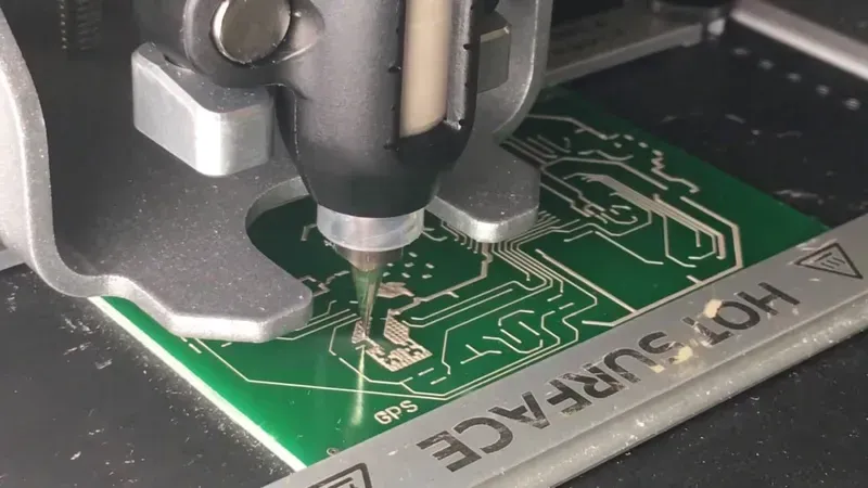
In today's rapidly evolving industrial landscape, maintaining optimal factory environments is paramount for operational efficiency, worker safety, and regulatory compliance. The proliferation of Industrial IoT (IIoT) has revolutionized how factories monitor critical parameters, from temperature and humidity to air quality and vibration. But what underpins the reliability and accuracy of these advanced monitoring systems? The answer lies in their foundational electronics: the Printed Circuit Boards (PCBs). This article delves into how Zero One Solution Limited provides comprehensive PCB solutions specifically tailored for factory environment monitoring sensors, ensuring robust performance and accelerating your path to smarter, safer industrial operations.
The Criticality of Factory Environment Monitoring
In the contemporary industrial landscape, the meticulous monitoring of factory environments transcends mere compliance, emerging as a foundational pillar for operational resilience, safety assurance, and optimized productivity. Real-time data on parameters such as temperature, humidity, air quality, vibration, and noise levels is indispensable, offering critical insights that drive proactive decision-making, prevent costly downtime, and foster a safer working atmosphere. This proactive approach, underpinned by advanced sensor PCB solutions, is vital for safeguarding assets, ensuring product quality, and enabling sophisticated predictive maintenance strategies that are the hallmark of Industry 4.0.
Safety & Compliance Enhancement Continuous monitoring of hazardous gases, extreme temperatures, and noise levels ensures adherence to stringent safety regulations and minimizes occupational risks. For instance, according to OSHA, maintaining proper ventilation and air quality is paramount for worker health, directly impacting productivity and reducing workplace incidents. Sensor-equipped PCBs provide the granular data needed to uphold these standards proactively.
Operational Efficiency & Quality Control Precise environmental control is critical for sensitive manufacturing processes, preventing material degradation, machinery malfunction, and compromised product quality. For example, in electronics manufacturing, uncontrolled humidity can lead to static discharge and material damage, while temperature fluctuations affect solder paste integrity. Environmental sensors, integrated via robust PCBs, enable immediate adjustments, ensuring consistent production parameters and reducing scrap rates.
Predictive Maintenance & Asset Longevity Beyond reactive repairs, environmental data facilitates predictive maintenance. Monitoring vibrations, thermal signatures, and humidity near machinery can detect early signs of wear or impending failure, allowing for scheduled interventions before critical breakdowns occur. This extends equipment lifespan, minimizes unscheduled downtime, and significantly reduces maintenance costs, enhancing overall operational continuity.
Common Challenges in Industrial Sensor Deployment
Deploying sensor systems in factory environments presents a unique array of challenges that go beyond typical electronics applications, fundamentally impacting sensor performance and the reliability of the underlying PCBs. Unlike controlled office settings, industrial spaces are characterized by dynamic and often harsh conditions. Overcoming these hurdles is paramount for ensuring accurate data collection and the long-term operational integrity of monitoring solutions, forming the bedrock for effective factory environment monitoring sensor PCB solutions.
Electromagnetic Interference (EMI) Industrial environments are rife with electrical machinery, motors, and power lines that generate significant electromagnetic interference. This EMI can corrupt sensor signals, leading to inaccurate readings or complete data loss, necessitating robust PCB design with proper grounding, shielding, and component placement to mitigate its effects. In 2022, studies indicated that EMI issues accounted for approximately 15% of reported sensor malfunctions in manufacturing facilities, highlighting its pervasive nature and impact on factory environment monitoring sensor PCB solutions. Zero One Solution leverages advanced signal integrity analysis and multilayer PCB designs to counter these challenges effectively, ensuring clean data transmission for Factory Environment Monitoring Sensor PCB Solutions.
Extreme Temperatures Factories can experience wide temperature fluctuations, from intense heat near furnaces to freezing conditions in cold storage. These extremes can degrade standard PCB materials, compromise solder joints, and affect the calibration and lifespan of sensors. Specialized high-Tg (glass transition temperature) laminates and thermally robust components are essential for maintaining performance. Data from industrial sensor failures show that temperature-related stress is a leading cause of premature aging and malfunction, directly impacting the reliability of factory environment monitoring sensor PCB solutions.
Vibrations and Mechanical Stress Heavy machinery, conveyor belts, and robotic systems generate constant vibrations that can exert significant mechanical stress on PCBs and sensor assemblies. This can lead to solder joint fatigue, component detachment, or even board cracks. Designing PCBs with reinforced mounting points, flexible substrates, and strategically placed, robust components is crucial for durability. According to a 2021 industrial equipment maintenance report, mechanical stress and vibration contributed to over 10% of sensor system failures, underscoring the need for resilient Factory Environment Monitoring Sensor PCB Solutions.
Addressing these multifaceted challenges requires a holistic approach to PCB design and manufacturing, focusing on material selection, layout optimization, and rigorous testing. Ignoring these factors can lead to frequent system failures, costly downtime, and unreliable data, undermining the entire purpose of factory environment monitoring.
The Indispensable Role of PCBs in Sensor Technology
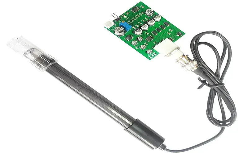
Sensor PCB Circuit Board
Printed Circuit Boards (PCBs) are the unseen, yet indispensable, technological bedrock upon which all modern factory environment monitoring sensor solutions are built. Far beyond mere conduits for electrical signals, PCBs act as the sophisticated central nervous system, meticulously integrating diverse sensor components, microcontrollers, communication modules, and power management units into a cohesive and functional monitoring device. Their precise layout and material selection are critical in ensuring the accuracy, reliability, and longevity of sensors operating within the demanding conditions of industrial environments, directly impacting data integrity and operational efficiency.
Component Integration Platform PCBs provide the physical platform for mounting and electrically connecting a multitude of components, including the sensor transducer itself (e.g., thermistor, humidity sensor, gas sensor), analog-to-digital converters (ADCs), microcontrollers for data processing, memory units, and power regulators. This systematic integration ensures optimal signal integrity and minimal interference, which is paramount for accurate data acquisition in noisy industrial settings.
Signal Routing and Conditioning The intricate traces on a PCB are precisely engineered to route sensitive analog and digital signals between components with minimal loss and distortion. For factory sensors, this often involves sophisticated signal conditioning circuits to amplify weak sensor outputs, filter out noise, and convert signals into a usable format for the microcontroller, ensuring that the collected environmental data is clean and reliable for analysis and decision-making.
Power Management Foundation Effective power management is crucial for the continuous operation of factory sensors, especially in remote or wirelessly connected devices. PCBs incorporate dedicated power management circuits, including voltage regulators, power filters, and battery management systems, to ensure stable and efficient power delivery to all sensor components. This design is vital for prolonging battery life in wireless sensors and maintaining consistent performance under varying power supply conditions.
Designing Robust PCBs for Harsh Factory Environments
Rugged PCB Manufacturing
The operational integrity and longevity of factory environment monitoring sensor PCBs hinge critically on their design and the materials chosen, particularly when facing the rigors of industrial settings. To ensure unwavering accuracy and reliability, these PCBs must be engineered to withstand a barrage of environmental stressors, including extreme temperatures, humidity, vibrations, corrosive agents, and electromagnetic interference. A robust design strategy integrates advanced material selection, protective coatings, precise impedance control, and highly effective thermal management, transforming potential vulnerabilities into resilient, high-performance monitoring solutions.
Durable Material Selection For factory environment monitoring PCBs, selecting substrates like high-Tg FR-4, polyimide, or ceramic-filled laminates is crucial. These materials offer superior thermal stability, chemical resistance, and mechanical strength compared to standard FR-4, ensuring the PCB maintains its structural and electrical integrity under harsh industrial conditions. For instance, high-Tg (glass transition temperature) laminates resist delamination and thermal stress better in high-temperature operations, a common challenge in manufacturing facilities.
Conformal Coating Application Conformal coatings (e.g., acrylic, silicone, epoxy, or urethane) provide a protective barrier against moisture, dust, chemicals, and corrosive gases prevalent in factory environments. This thin polymeric film extends the lifespan of the PCB by preventing short circuits and corrosion on sensitive components, making it an indispensable layer of defense for sensor electronics.
Effective Thermal Management Heat dissipation is paramount for sensor PCBs, especially those operating continuously or processing high data volumes. Design techniques include incorporating thermal vias, copper pours, heat sinks, and even specialized thermal management laminates. Efficient thermal pathways prevent localized hotspots, which can degrade component performance, reduce sensor accuracy, and ultimately lead to premature failure. For example, a 10°C reduction in operating temperature can often double the lifespan of electronic components.
Impedance Control for Signal Integrity Maintaining consistent impedance in high-speed signal traces is vital for accurate data transmission from sensors. Variations in trace width, dielectric constant, or ground plane integrity can lead to signal reflections and data corruption. Rigorous impedance control, often achieved through precise trace routing and material selection, ensures the integrity of sensor data, which is critical for reliable factory environment monitoring.
Vibration and Mechanical Shock Resistance Factory environments often expose PCBs to constant vibrations and potential mechanical shocks. Designing for robustness includes employing robust component mounting techniques (e.g., through-hole components, optimized solder pads), incorporating internal stress relief features, and utilizing thicker copper layers for enhanced structural stability. These measures mitigate the risk of solder joint fatigue and component dislodgement, preserving sensor functionality.
Zero One Solution's Comprehensive PCB Services for Sensor Applications
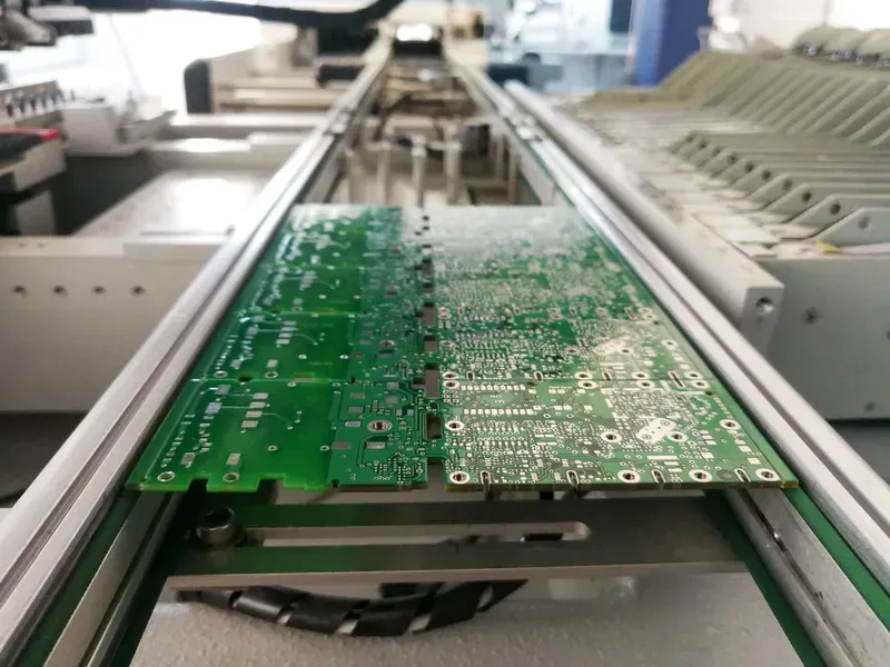
Factory PCB Production Line
Zero One Solution Limited stands as a veteran leader in providing end-to-end PCB services, meticulously tailored for the exacting demands of Factory Environment Monitoring Sensor PCB Solution. Our holistic approach, encompassing rapid prototyping, expert PCB design optimization, precision manufacturing, and efficient assembly, is engineered to empower industrial innovators in swiftly bringing their advanced sensor technologies to market with unparalleled reliability and performance. We understand that the foundation of any robust sensor system lies in its underlying PCB, and our comprehensive capabilities ensure that this foundation is not just strong, but optimized for the challenging operational realities of factory environments.
Rapid Prototyping for Accelerated Development Our rapid prototyping services significantly reduce development cycles, allowing engineers to quickly test and iterate on their sensor PCB designs. This agility is crucial in the fast-paced industrial IoT sector, enabling faster validation and refinement of complex sensor architectures.
Expert PCB Design Optimization Beyond mere fabrication, our seasoned design engineers specialize in optimizing PCB layouts for sensor applications. This includes meticulous consideration of signal integrity, power efficiency, EMI suppression, and component placement to ensure peak sensor performance and longevity in industrial settings.
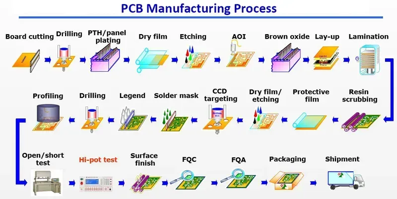
Precision Manufacturing Capabilities Leveraging state-of-the-art manufacturing facilities, Zero One Solution delivers high-precision PCBs built to withstand harsh factory conditions. We employ advanced fabrication techniques and quality control measures to ensure every board meets stringent industry standards for durability and functionality.
Efficient & Reliable Assembly Services Our in-house PCB assembly services provide a seamless transition from manufacturing to a fully functional sensor module. With advanced SMT and THT capabilities, we ensure precise component placement and soldering, reducing post-assembly defects and accelerating time-to-market for your monitoring solutions.
Service Aspect
Zero One Solution Advantage
Impact on Sensor PCB Projects
Design Review & DFM
Proactive identification of manufacturability issues, cost reduction opportunities.
Minimizes costly redesigns, accelerates production readiness, enhances reliability.
Material Selection Guidance
Expert advice on optimal substrates (e.g., Rogers, high-Tg FR-4) for specific environmental stresses.
Ensures thermal stability, chemical resistance, and long-term performance.
Conformal Coating Application
Precision application of protective coatings against moisture, dust, and chemicals.
Extends lifespan and maintains sensor accuracy in harsh industrial conditions.
Strict Quality Control
Multi-stage inspection (AOI, X-ray, ICT) and rigorous testing protocols.
Guarantees defect-free boards, reduces field failures, and ensures compliance.
Global Supply Chain Management
Strategic sourcing of components and materials through a robust global network.
Ensures stable supply, competitive pricing, and reduced lead times for critical parts.
Tailored PCB Solutions for Diverse Industrial Monitoring Needs
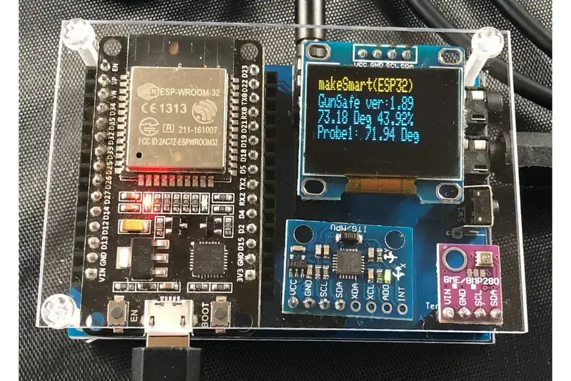
Multi-Sensor Integration PCB
At Zero One Solution Limited, we understand that no two factory environments are identical, and thus, off-the-shelf PCB solutions rarely meet the intricate demands of sophisticated industrial monitoring. Our core strength lies in providing highly tailored PCB solutions that precisely align with the specific sensor types and communication protocols critical for your unique industrial monitoring needs. This bespoke approach ensures optimal performance, seamless data integration, and maximum operational longevity within even the most challenging factory settings.
Customization for Various Sensor Types We offer extensive customization for PCBs integrating a wide array of sensors essential for comprehensive factory environment monitoring. This includes, but is not limited to, gas sensors for detecting harmful chemicals, pressure sensors for pipeline and pneumatic systems, vibration sensors for machinery health monitoring, and sound sensors for anomaly detection or noise level compliance. Our design expertise ensures proper signal conditioning, noise reduction, and power delivery for each sensor type, maximizing accuracy and reliability.
Seamless Integration with Industrial Communication Protocols Beyond sensor integration, our tailored PCB solutions prioritize seamless connectivity. We design PCBs to facilitate robust communication across diverse industrial protocols, ensuring your monitoring system integrates effortlessly with existing infrastructure. This includes popular wireless standards like Wi-Fi for localized data transfer and LoRa for long-range, low-power applications, as well as wired protocols such as Ethernet for high-bandwidth data and Modbus for industrial control systems. This versatility guarantees reliable data transmission from the sensor edge to your control room or cloud-based analytics platforms.
Optimized for Specific Environmental Challenges Recognizing the harsh realities of factory environments, our custom PCB designs incorporate features that mitigate common industrial challenges. This involves selecting specialized substrates for high-temperature resilience, applying conformal coatings for protection against humidity and corrosive agents, and employing robust layout strategies to minimize electromagnetic interference (EMI). Each tailored solution is engineered to withstand the specific stressors of your operational environment, ensuring sustained performance and minimal downtime.
Sensor Type
Typical Application
Key PCB Design Consideration
Gas Sensor
Leak detection, air quality monitoring
Analog frontend precision, power efficiency, environmental protection
Pressure Sensor
Hydraulic/pneumatic system monitoring, flow control
Accelerating Innovation with Rapid Prototyping and DFM Expertise
PCB Rapid Prototyping
In the fast-paced world of industrial IoT and factory automation, the speed of innovation directly impacts market leadership. Zero One Solution Limited stands as a pivotal partner for companies developing factory environment monitoring sensor solutions, offering unparalleled rapid prototyping services. Our ability to quickly transform a concept into a tangible, functional PCB prototype is a critical differentiator, dramatically shortening development cycles and enabling rapid iteration. This agility, coupled with our rigorous Design-for-Manufacturability (DFM) expertise, ensures that initial designs are not only functional but also optimized for cost-effective, high-volume production, translating directly into a faster time-to-market and a superior final product.
Reduced Development Timelines Our rapid prototyping capabilities allow engineers to test and validate their sensor PCB designs quickly. This iterative approach means that design flaws are identified and corrected early in the process, significantly reducing the overall time from concept to commercialization. For complex factory monitoring systems, this speed is invaluable, as it enables companies to respond to evolving market demands and technological advancements with unprecedented agility.
Cost Efficiency Through DFM Integrating DFM principles from the outset is crucial for the long-term economic viability of any sensor product. Our DFM expertise goes beyond mere design validation; we meticulously analyze each PCB layout to identify potential manufacturing hurdles, optimize material usage, and streamline assembly processes. This proactive approach minimizes costly re-spins, reduces scrap rates, and ensures that the transition from prototype to mass production is smooth and economical, yielding significant savings over the product's lifecycle.
Enhanced Product Reliability Early and frequent prototyping, combined with DFM analysis, leads to a more robust and reliable final product. By simulating real-world factory conditions during the prototyping phase and optimizing component placement and thermal management through DFM, we help clients build highly resilient sensor PCBs that can withstand harsh industrial environments. This focus on reliability translates into fewer field failures, lower maintenance costs, and increased operational uptime for the end-user.
Competitive Market Advantage The ability to rapidly innovate and efficiently bring new factory environment monitoring sensor solutions to market provides a substantial competitive edge. Companies leveraging Zero One Solution's rapid prototyping and DFM services can outpace competitors, capture market share quicker, and establish themselves as leaders in the industrial automation sector. Our strategic location in Shenzhen and global network further accelerate supply chain efficiencies.
/* Example of DFM considerations for a sensor PCB */
function analyzeDFM(pcbDesign) {
  let issues = [];
  // Check for component spacing violations
  if (pcbDesign.componentSpacing < 0.2) {
    issues.push("Component spacing too tight for automated assembly.");
  }
  // Evaluate trace width for current handling
  if (pcbDesign.traceWidth < 0.15 && pcbDesign.currentDraw > 1.0) {
    issues.push("Insufficient trace width for expected current.");
  }
  // Assess via tenting for environmental protection
  if (!pcbDesign.viaTenting) {
    issues.push("Consider via tenting for improved environmental resistance.");
  }
  return issues;
}
Frequently Asked Questions about Sensor PCBs for Factory Monitoring
What are the optimal PCB material selections for sensor PCBs in harsh factory environments? For sensor PCBs operating in harsh factory environments, optimal material selection is crucial. High-Tg (glass transition temperature) laminates such as FR-4 variants like Isola 370HR or Panasonic Megtron 6 are often preferred for their enhanced thermal stability. For environments with high humidity or chemical exposure, materials with low moisture absorption and chemical resistance, such as PTFE-based laminates (e.g., Rogers RO4000 series), are recommended. Additionally, copper foil adhesion strength and low Dk/Df (dielectric constant/dissipation factor) values are considered for signal integrity in high-frequency sensor applications, ensuring reliable data transmission under challenging conditions. The choice ultimately balances thermal, mechanical, and electrical performance requirements against the specific environmental stressors of the factory.
How are reliability testing procedures conducted for industrial sensor PCBs? Reliability testing for industrial sensor PCBs is rigorous and comprehensive, designed to simulate operational stresses and ensure long-term performance. Key tests include Highly Accelerated Life Testing (HALT) and Highly Accelerated Stress Screening (HASS) to identify design weaknesses and potential failure modes. Environmental tests encompass thermal cycling (simulating temperature fluctuations), humidity exposure, vibration testing (to assess mechanical robustness), and shock testing. Electrical tests include functional testing across extreme operating parameters, impedance control verification, and insulation resistance testing. These procedures adhere to industry standards like IPC-A-610 and J-STD-001, providing empirical data on a PCB's durability and suitability for its intended industrial application, minimizing costly field failures.
Are custom PCB solutions cost-effective for factory environment monitoring sensors? While custom PCB solutions for factory environment monitoring sensors may incur higher initial design and tooling costs compared to off-the-shelf options, they prove highly cost-effective in the long run. Customization allows for precise optimization of size, performance, and integration with specific sensor types and industrial protocols, leading to reduced overall system complexity, fewer components, and enhanced reliability. This optimization translates to lower assembly costs, improved power efficiency, and extended product lifespan, ultimately minimizing maintenance and replacement expenditures. For specialized industrial applications where standard solutions fall short, custom PCBs offer a superior return on investment by providing tailored performance and unparalleled stability.
What are the typical lead times for industrial sensor PCB projects, from design to delivery? Typical lead times for industrial sensor PCB projects vary significantly based on project complexity, order volume, and the scope of services required. For rapid prototyping and R&D samples, lead times can be as short as 3-7 business days for bare PCBs, with full assembly adding another 5-10 days. For medium-to-high volume production runs, the entire process, from finalized design to delivery, typically ranges from 3 to 6 weeks. This includes time for material procurement, manufacturing, quality control, assembly, and final testing. Factors such as specialized material availability, component lead times, and the intricacy of the PCB design can influence the overall timeline, necessitating close collaboration with the PCB solution provider.
In conclusion, the efficacy and longevity of factory environment monitoring systems hinge significantly on the quality and reliability of their underlying PCB solutions. As industries move towards smarter, more connected operations, the demand for robust, high-performance sensor PCBs will only intensify. Zero One Solution Limited stands as your premier partner, combining two decades of Silicon Valley expertise with a global supply chain to deliver unparalleled rapid prototyping, custom design, manufacturing, and assembly services for your industrial sensor needs. Don't let PCB limitations hinder your innovation. Contact Zero One Solution today to discuss how our bespoke PCB solutions can elevate your factory environment monitoring systems and drive your industrial success.