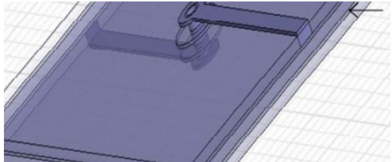
When a high-speed signal transitions between layers, omitting a nearby return via won't show up on the schematic, and the board may even power up and function normally. But once you reach higher edge rates, longer transmission lines, or EMI testing, the problems emerge — impedance dips, increased insertion loss, and radiation issues. The root cause is often not the signal via itself, but the fact that the return current did not transition layers along with the signal.
Many PCB design reviews focus only on the signal via's diameter, anti-pad, and stub, treating the nearby ground via as an optional "fill-where-possible" item. This approach may work at lower frequencies, but high-speed return currents do not cross reference planes without a low-impedance path.
The principle is straightforward: when the signal current changes layers, the return current must also have a low-impedance interlayer channel nearby. The farther the ground via is placed, the longer the return path, resulting in increased loop area and parasitic inductance.
A top-layer microstrip references the adjacent ground layer. When transitioning to an inner stripline layer, the reference may become a different ground layer or even a power plane. You cannot simply look at the routing layer — you must check the adjacent planes above and below and understand the actual return conditions for the frequency of interest.
If both layers reference the same continuous ground plane, the return transition is relatively low-risk
If the reference plane changes, ground vias or interplane decoupling capacitors become the critical path for return current transfer
Even with a local high-frequency connection between power and ground planes, the return path may still detour significantly
The via model — including pad diameter, drill diameter, anti-pad, and layer spacing — collectively defines the local interconnect structure. This reminds us that a via is not an ideal node, but a 3D interconnect with impedance and electric field distribution.
| Parameter | Typical Value |
|---|---|
| Pad Diameter | 400 μm |
| Via Diameter | 200 μm |
| Anti-Pad Diameter | 600 μm |
| Dielectric Thickness Between Layers | 100-200 μm |
These parameters collectively determine the parasitic inductance and capacitance of the via section. All must be considered together, rather than optimizing a single parameter in isolation.
Placing a ground via nearby shortens the lateral distance of the return path. For differential pairs transitioning layers, place return vias symmetrically on both sides to avoid asymmetry that converts differential-mode energy into common-mode noise.
"Close" must be defined in the context of your manufacturer's capabilities and the anti-pad boundaries:
Placing the ground via too close to the signal via may alter local capacitance due to interaction between the anti-pad and via pad
Placing it too far increases loop inductance and worsens impedance discontinuity
The optimal spacing should be determined through stackup and target impedance simulation, not by blindly following a fixed millimeter rule
Adding more ground vias yields diminishing returns beyond a certain point. Simulation data shows that both the number and spacing of ground vias affect S-parameters, but the relationship is not linear. Design priority should be ensuring the nearest effective return path, then considering additional fence vias.
The inductance of the via, the capacitance of the pad and anti-pad, combined with the detoured return path, create a local impedance discontinuity. In the time domain, this appears as a brief dip or peak; in the frequency domain, it manifests as increased reflection and insertion loss.
Simply making the signal via smaller does not necessarily solve the problem. If the return path still must route to a distant ground via, the dominant loop inductance has not been reduced. Instead, optimizing ground via placement, plane openings, and the transition structure is often more effective than modifying the signal via alone.
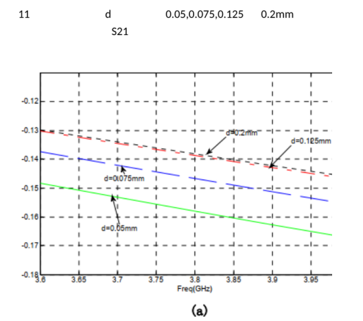
For simulation or testing, always model the signal via, ground via, and the actual reference planes together. Extracting a single isolated signal via will miss the critical return boundary condition, and the resulting impedance data will not reliably guide layout decisions.
During high-speed PCB design reviews, we recommend a systematic process to check return paths:
Identify every layer transition along the entire high-speed link
Document the reference plane (ground or power) before and after each transition
Measure the distance to the nearest ground via or interplane decoupling capacitor
Verify that the return path is not blocked by slots, plane splits, or anti-pad cutouts
If the board is already populated, use TDR (Time-Domain Reflectometry) to locate impedance variations near transitions, and compare S-parameters across different return via configurations. For spectrum-related issues, monitor cable common-mode current or near-field strength to see if they improve with ground via optimization.
During review, don't just ask: "Are there ground vias next to the signal?" Instead, ask:
Does this ground via actually connect to both reference planes? Is the distance reasonable? Is the return still forced to cross a large anti-pad area?
This line of questioning aligns more closely with the actual physical behavior of return currents.
When a signal moves from a layer referenced to a power plane to one referenced to a ground plane, the true high-frequency return path may be through a local decoupling capacitor. If that capacitor is too far from the transition point, the return current will detour laterally across the plane, increasing loop inductance.
Ground via fences near board edges or connectors serve to control field boundaries and suppress radiation. The transition point needs a directly adjacent low-impedance connection for that specific layer change. The two serve different functions and their placement rules are not interchangeable.
If a signal crosses a reference plane split, even with nearby ground vias, the return current may not be able to reach the other side. The preferred fix is to reroute the signal or restore a continuous plane. If using a thin copper bridge as a patch, its high-frequency impedance must be evaluated — DC continuity alone does not guarantee adequate high-speed performance.
Under ideal symmetric conditions, differential return currents partially cancel. However, they still couple to the reference plane. If the two lines have asymmetric transition structures, ground vias on only one side, or significant differences in via-to-line spacing, the result is conversion of differential-mode energy into common-mode, leading to EMI issues.
When space is tight in the connector escape region, prioritize the signal via and the closest return via before routing lower-speed nets. If you wait until all traces are routed before adding ground vias, you will often be left with positions too far from the signal or options that disrupt the reference plane — making later fixes more costly.
Before production, add return via net names, via types, and solder mask requirements to your design rule checklists. This prevents them from being accidentally removed or modified during panelization, version migration, or library updates. If high-speed design rules rely solely on engineer memory, they are likely to be overlooked in the next revision.
A high-speed signal layer transition is not an action performed by the signal trace alone — it is a layer transition completed jointly by the signal and its return current. Treating the return via as an optional or secondary element means completing only half the interconnect.
On your next high-speed via review, start by tracing the complete return loop around the reference planes, then determine the distance, number, and anti-pad design for your return vias. If the return path doesn't close cleanly, impedance and EMI issues will eventually reveal the oversight — often at the worst possible time.
Let AnyPCBA Help You Mitigate "Hidden" High-Speed Design Risks
In high-speed PCB design, return path issues, via optimization, and stackup choices often go unnoticed during prototyping — only surfacing during production or EMI testing, when fixes are expensive and time-consuming.
AnyPCBA's engineering team provides DFM/DFA design reviews during the design phase, covering return via placement, reference plane integrity, signal integrity, and other critical dimensions. If you're facing design challenges with high-speed interfaces (DDR, PCIe, SerDes), multilayer boards, or complex layer transitions, we're here to help.
Contact our engineering team →




