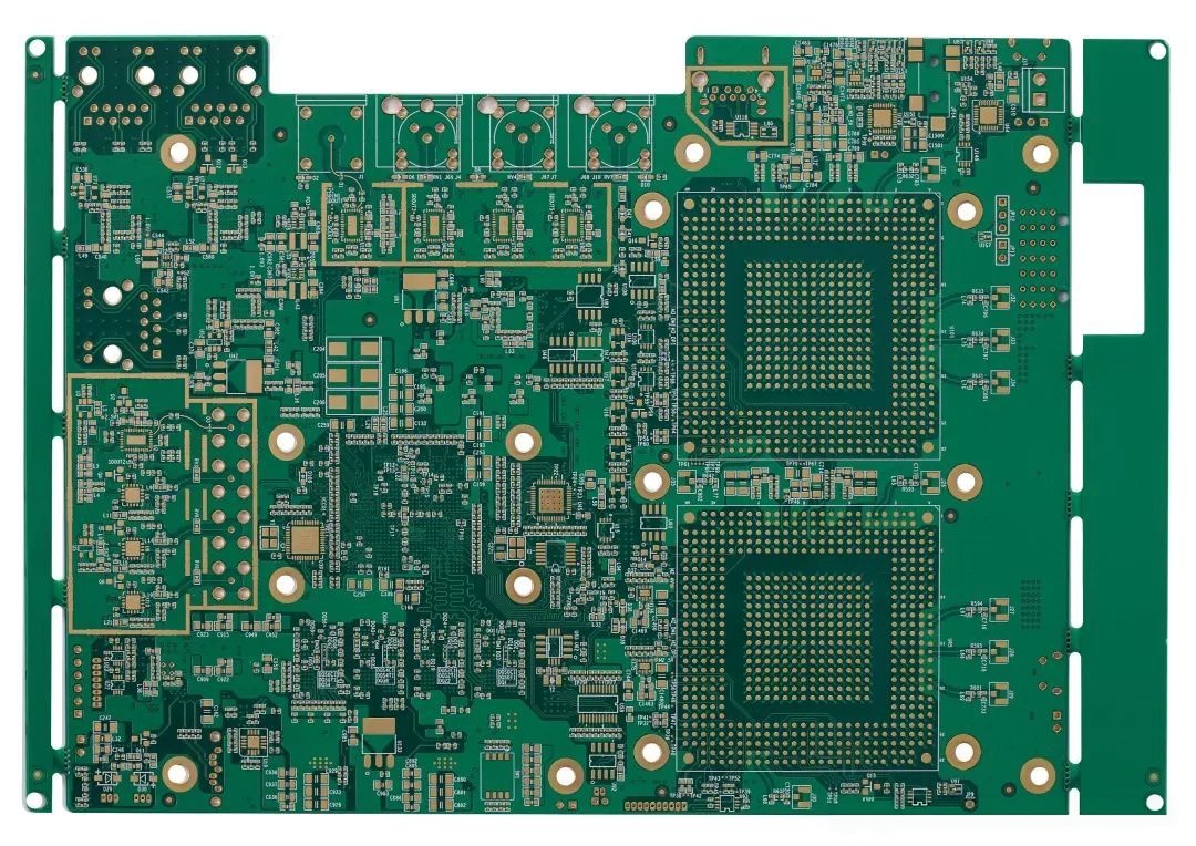
In high-end electronics manufacturing, 8-layer PCBs have become the core substrate for applications such as 5G communications, AI servers, and automotive electronics, owing to their superior signal integrity and complex circuit carrying capacity. Their performance is highly dependent on precise lamination processes, which involve material science, thermal management, and electromagnetic compatibility.
This article provides a systematic analysis of 8-layer PCB lamination technology from three perspectives: structural design logic, key process control elements, and typical challenges with solutions.
The core advantage of an 8-layer PCB comes from the scientific planning of its layer stackup. A typical symmetrical stackup follows a configuration such as "Signal-Ground-Signal-Power-Core-Power-Signal-Ground". This architecture delivers performance optimization through the following mechanisms:
Electromagnetic Isolation: Inner ground and power planes form a Faraday cage structure, surrounding high-speed signal layers (such as PCIe 5.0 differential pairs) to effectively suppress crosstalk and electromagnetic radiation. Test data shows this design can reduce signal loss by 40% at 10GHz.
Power Integrity: Dedicated power planes combined with a decoupling capacitor network can keep power noise within ±5mV, meeting the power supply requirements of high-density chips like FPGAs.
Thermal Optimization: Differential copper thickness design (e.g., 3oz on outer layers, 1oz on inner layers) combined with thermal via arrays (density ≥ 4/cm²) can reduce chip junction temperature by 18°C.
The lamination process is the core of 8-layer PCB manufacturing, requiring precise control across material, temperature, and pressure dimensions:
High-frequency applications prioritize substrates with low dielectric loss (Df < 0.002), such as Rogers RO4350B or Isola 370HR, paired with HVLP copper foil (surface roughness ≤ 1μm) to reduce skin effect loss by 30% for signals above 10GHz. The resin content of prepregs must be strictly matched to the substrate; for example, prepregs with Tg ≥ 170°C ensure interlayer stability in extreme environments from -55°C to 150°C.
Temperature Profile: A three-stage heating strategy (pre-heat at 120°C → soak at 180°C → cool at 80°C) with temperature gradient control within ±2°C prevents thickness deviation caused by excessive resin flow.
Pressure Management: Dynamic pressure of 350psi ±10% achieves copper-to-dielectric peel strength of 1.8N/mm (industry average 1.2N/mm), significantly improving long-term reliability.
Vacuum Environment: Vacuum degassing (vacuum level ≤ -0.1MPa) during lamination keeps interlayer void rates below 0.01%, eliminating potential risks in high-frequency signal transmission.
Interlayer registration deviation for 8-layer boards must be controlled within ±25μm. Advanced manufacturing employs laser positioning systems (accuracy ±5μm) and AI vision inspection to achieve closed-loop control from drilling to lamination, ensuring blind/buried via reliability ≥ 99.99%.
For 5G millimeter-wave bands (24GHz and above), hybrid dielectric design is required: signal layers using PTFE-based substrates (Dk=2.1) and power layers using FR-4 (Dk=4.3). Stackup optimization through ANSYS HFSS simulation can reduce insertion loss to below 0.5dB/cm. Additionally, back-drilling technology eliminates via stubs (Stub Length ≤ 0.2mm) to prevent signal reflections.
The multilayer structure of 8-layer boards is prone to warping during thermal cycling. Using low-CTE materials (coefficient of thermal expansion ≤ 15ppm/°C) combined with symmetrical stackup design can control warpage within 0.05mm/m.
The dual assurance of precision AOI optical inspection (5μm resolution) and flying probe testing (contact resistance ≤ 50mΩ) maintains electrical performance yields above 98% for 8-layer boards. In one military radar project, this approach integrated 2000+ components on an 80mm×60mm board, improving yield from 60% to 98%.
AnyPCBA has over a decade of experience in PCB manufacturing, enabling efficient and precise 8-layer board production through a "Materials Science + Intelligent Engineering + Application-Specific Development" technology framework:
Intelligent Lamination Line: Adaptive lamination systems support fast changeovers from 2 to 64 layers, with real-time pressure feedback ensuring interlayer thickness variation ≤ 3% to meet tight tolerances of high-end applications.
Material and Process Adaptability: For high-reliability automotive electronics, AnyPCBA uses secondary curing processes to raise FR-4's glass transition temperature. Combined with ENIG surface finish, this extends board life under 125°C high-temperature conditions. In 5G base station projects, precise hybrid lamination of Rogers materials with FR-4 achieves insertion loss at 28GHz better than the industry average.
Precision Manufacturing and Quality Control: AnyPCBA's laser drilling technology processes micro-vias with wall roughness Ra ≤ 2.5μm, while fully automated X-Ray layer registration inspection ensures multi-layer alignment accuracy. Manufacturing strictly follows IPC-6012 Class 3 standards, with full traceability from raw materials to finished products.
8-layer PCB manufacturing is the result of collaborative innovation in materials, design, and process. As electronic devices evolve toward higher frequencies and smaller form factors, breakthroughs in lamination technology will continue to be a key driver of industry progress. Through the deep integration of technical expertise and smart manufacturing, AnyPCBA provides full-chain support from prototyping to production, ensuring reliable delivery of high-end electronic products.
Need High-Layer-Count PCB Manufacturing Support?
AnyPCBA has extensive experience in multilayer PCB manufacturing, supporting 2-64 layers including HDI, rigid-flex, high-frequency hybrid, and heavy copper processes for high-reliability applications in automotive, 5G, AI server, and medical equipment sectors.
Contact us to learn more →




