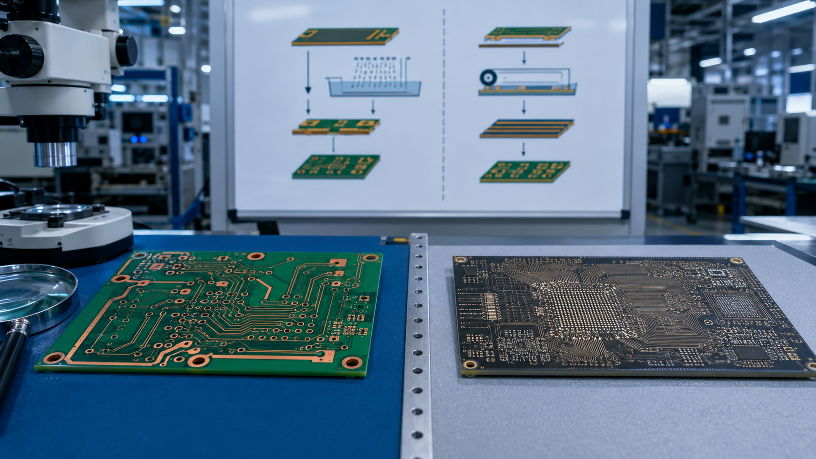
As electronic products continue to evolve toward higher density, thinner profiles, and greater performance, PCB manufacturing technology faces new challenges and opportunities. Among the many process routes, subtractive and additive are the two core technology paths, each with significant differences in principle, cost, and application scenarios.
This guide provides a systematic, in-depth comparison to help you choose the most suitable manufacturing process for your project.
The subtractive process starts with copper-clad laminate and removes unwanted copper through chemical etching to retain the desired circuit pattern.
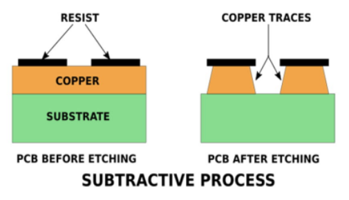
Key Steps:
Cutting and surface preparation of copper-clad laminate
Pattern transfer (lamination, exposure, development)
Removal of excess copper foil using acid/alkaline etchant
Solder mask and legend printing
Characteristics: Relies on "subtracting" copper to form conductive paths. Requires precise control of etching parameters to avoid over-etching or copper residue.
The additive process deposits conductive materials (such as copper or silver paste) directly onto an insulating substrate, building circuits layer by layer.
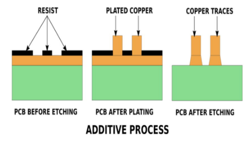
Key Steps:
Pretreatment of bare substrate (e.g., polyimide, ceramic)
Selective application of photoresist or electroplating to deposit conductive layers
Drying, curing, and removal of excess material
Characteristics: No etching required, enabling fine-line circuits suitable for micro-pitch and high-density designs.
| Step | Subtractive Process | Additive Process |
|---|---|---|
| Material Preparation | Copper-clad laminate (copper foil + resin substrate) | Bare substrate (e.g., polyimide film, ceramic) |
| Pattern Transfer | Photoresist coating → Exposure → Development | Photoresist coating → Exposure → Development |
| Circuit Formation | Etching → Reducing copper thickness | Electroplating → Adding conductive material |
| Post-Processing | Solder mask, surface finish (OSP/HASL/ENIG) | Solder mask, surface finish (OSP/HASL/ENIG) |
Typical Applications:
Subtractive: Consumer electronics motherboards, home appliance control boards, automotive electronics modules
Additive: Flexible medical sensors, high-frequency microwave substrates, semiconductor packaging substrates
Strengths:
High Technical Maturity: Over 80% market share with a well-established supply chain
Cost-Effective for High Volume: Suitable for large-scale production of single/double-sided and multilayer boards
Excellent Thermal Performance: Thicker copper layers support high-current applications
Broad Material Selection: Supports FR-4, high-frequency materials, metal-core boards, and more
Limitations:
Environmental Concerns: High cost of etching wastewater treatment
Line Width/Spacing Limits: Practical limit around 20μm, not suitable for ultra-high-density
Poor Flexibility: Not suitable for foldable or wearable devices
Strengths:
Ultra-Fine Line Capability: Line width below 5μm, supporting IC substrate-level precision
Environmentally Friendly: No copper etching waste, more sustainable
Complex Structure Support: Enables 3D curved and through-hole circuits
Special Substrate Compatibility: Suitable for ceramic, polyimide, and other non-metallic substrates
Limitations:
High Equipment Cost: Expensive electroplating and vacuum deposition equipment
Material Constraints: Primarily used with non-metallic substrates (ceramic, polymer)
Lower Volume Efficiency: Better suited for small-batch production and high-value applications
Fixed Costs: Etching and exposure equipment depreciation (approximately 30% of total cost)
Variable Costs:
Copper waste: Higher waste rate with finer line widths
Etchant consumption: Ongoing chemical consumption
Wastewater treatment: Environmental compliance costs
Typical Cost Estimate (1㎡ 4-layer FR-4 board, 100μm line width):
Material cost: ~$12
Processing cost: ~$8 (includes etching, drilling)
Total: ~$20
Fixed Costs: Electroplating equipment, cleanroom maintenance (approximately 45% of total cost)
Variable Costs:
Conductive materials: High cost of nano-silver paste and other precious metals
Energy consumption: Significant power usage for electroplating and sputtering
Yield loss: Lower yield for complex structures
Typical Cost Estimate (1㎡ 6-layer ceramic substrate, 20μm line width):
Material cost: ~$35
Processing cost: ~$18 (includes sputtering, electroplating)
Total: ~$53
| Volume Scale | Cost Comparison |
|---|---|
| High Volume (>500㎡) | Subtractive is approximately 35% lower |
| Low Volume (<100㎡) | Additive premium can reach 200% |
Key Takeaway: For high-volume orders, subtractive offers significant cost advantages. For low-volume, high-precision requirements, additive delivers capabilities that subtractive cannot achieve.
| Scenario | Recommended Process | Key Reason |
|---|---|---|
| Consumer Electronics Motherboards | Subtractive | High volume, low cost, mature technology |
| 5G Base Station High-Frequency PCBs | Additive | Low dielectric loss, supports millimeter-wave frequencies |
| Wearable Device Flex Circuits | Additive | Bend cycles > 100,000, thickness < 0.1mm |
| Automotive Control Modules | Subtractive | High-temperature resistance (150°C), vibration resistance |
| Semiconductor Package Substrates | Additive | Line width/spacing ≤ 50μm |
| Military/Aerospace High-Reliability PCBs | Subtractive | Proven reliability standards |
Laser Direct Structuring (LDS): Selective copper plating enabled by laser activation
Green Etchants: More environmentally friendly etching systems
Roll-to-Roll (R2R) Production: Continuous manufacturing for flexible substrates
3D Printed Conductive Inks: Nano-silver/copper particles direct printing with 10μm precision
Subtractive + Additive Combination: Main circuits using subtractive, micro-vias using additive
Selective Additive: Ultra-high-density interconnects in key areas while maintaining cost advantages elsewhere
Choosing the right PCB manufacturing process ultimately involves balancing cost, precision, and volume:
| Decision Factor | Subtractive Priority | Additive Priority |
|---|---|---|
| Volume | High volume (>500㎡) | Low volume, prototyping |
| Precision | Line width > 50μm | Line width < 50μm |
| Substrate Type | FR-4, metal-core, standard materials | Ceramic, polyimide, specialty materials |
| Cost Sensitivity | High | Low |
| Environmental Requirements | Standard | High (no etching waste) |
For engineers, understanding the characteristics and application scenarios of both processes is essential for tackling next-generation electronic product challenges.
Need Help Choosing the Right PCB Process for Your Project?
AnyPCBA has over a decade of experience in PCB manufacturing, supporting both subtractive and additive process routes across 2-64 layers. Our engineering team provides DFM/DFA design reviews to help you evaluate the cost, lead time, and performance implications of different process options.
Contact us to discuss your project →




