In an era increasingly powered by renewable energy, Home Energy Storage Systems (HESS) are pivotal, offering sustainable and reliable power to households. The heart of these sophisticated systems lies within their Printed Circuit Boards (PCBs). At Zero One Solution Limited, founded in 2011 and a leader in rapid-response R&D prototype manufacturing, we understand the critical role high-performance PCBs play in the efficiency and reliability of HESS. Our comprehensive PCB solutions, from design to manufacturing and assembly, are engineered to empower our clients to accelerate product development and bring groundbreaking energy solutions to market with unparalleled efficiency. How can a tailored PCB solution unlock the full potential of your next-generation home energy storage system?
The Rise of Home Energy Storage Systems and Their PCB Needs
The burgeoning adoption of Home Energy Storage Systems (HESS) marks a pivotal shift towards sustainable and resilient residential power, driven by the escalating demand for energy independence, grid stability, and renewable energy integration. At the heart of every robust HESS lies the Printed Circuit Board (PCB), serving as the foundational interconnected platform that orchestrates power conversion, battery management, and system control. The reliability, efficiency, and safety of these systems are intrinsically linked to the quality and precision of their PCB solutions, making advanced PCB design and manufacturing not merely a component, but a non-negotiable imperative for the future of home energy.
Demand Drivers for HESS The global HESS market is projected to reach USD 22.8 billion by 2030, growing at a CAGR of 17.5% from 2023. Key drivers include rising electricity costs, increasing renewable energy adoption (e.g., solar panels), governmental incentives, and the critical need for backup power during outages. Consumers seek to maximize self-consumption of renewable energy and reduce reliance on traditional grids, necessitating efficient storage solutions.
Why PCBs are Critical for HESS Functionality PCBs are the central nervous system of HESS, facilitating seamless communication and power flow between diverse components. They are essential for accurate battery monitoring, efficient power inversion (DC to AC), precise charge/discharge control, and the integration of smart home energy management systems. Without highly reliable PCBs, HESS cannot achieve optimal performance or ensure long-term operational stability.
Ensuring HESS Efficiency and Safety through PCBs High-quality PCBs are vital for minimizing energy losses within HESS, leading to greater overall system efficiency. Furthermore, they are paramount for safety protocols, enabling precise thermal management, overcharge/discharge protection, and fault detection. Advanced PCB designs incorporate features like robust copper traces for high current paths and specialized materials for thermal dissipation, directly contributing to the prevention of system failures and potential hazards.
Key PCB Components in Home Energy Storage
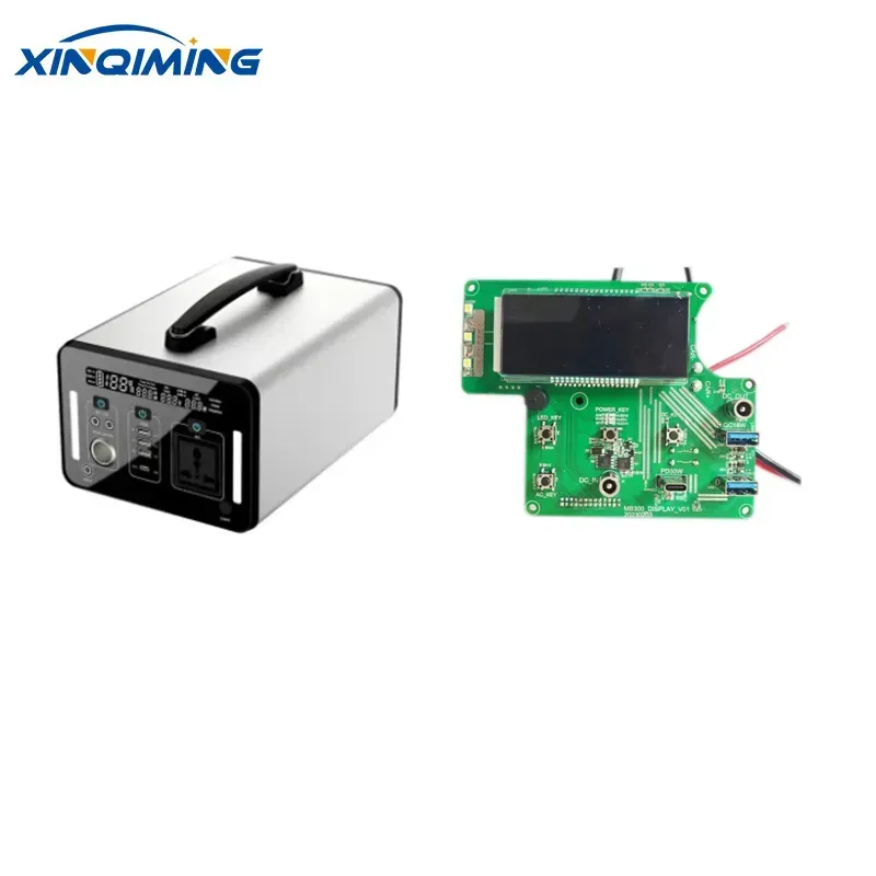
Home Energy Storage System PCB Board
At the core of every efficient Home Energy Storage System (HESS) lies a sophisticated network of Printed Circuit Boards (PCBs), each meticulously designed to manage, convert, and control energy flow. These specialized PCBs are not merely connectors; they are the intelligent backbone ensuring optimal performance, longevity, and crucial safety for residential energy independence. Understanding the distinct roles of Battery Management System (BMS) PCBs, inverter PCBs, and control unit PCBs is fundamental to appreciating the technological prowess required for robust HESS solutions.
PCB Component
Primary Function
Critical Role in HESS
Key Design Considerations
Battery Management System (BMS) PCB
Monitors and controls battery charge/discharge cycles, temperature, voltage, and current.
Prevents overcharging, deep discharge, and thermal runaway, extending battery life and ensuring safety.
High current handling, precision sensing, robust fault detection, thermal management, communication interfaces (CAN, I2C).
Inverter PCB
Converts DC power from batteries/solar panels into AC power for household use, and vice versa.
Enables seamless integration with the grid and household appliances, maximizing energy utilization.
High power density, efficient heat dissipation, robust EMI/EMC compliance, high-frequency operation, power switching component integration (IGBTs, MOSFETs).
Control Unit PCB
Serves as the central processing unit, managing system operations, data logging, and user interface.
Orchestrates the entire HESS, optimizing energy flow, responding to grid signals, and providing system diagnostics.
High processing power, multiple communication protocols (Ethernet, Wi-Fi, RS485), data storage, low power consumption, real-time operating system (RTOS) support.
Challenges in Designing HESS PCBs
Engineer Designing PCB Board
Designing Printed Circuit Boards (PCBs) for Home Energy Storage Systems (HESS) presents a complex array of challenges that demand specialized engineering expertise to ensure optimal performance, safety, and longevity. Unlike conventional electronics, HESS PCBs must endure extreme operational conditions, including high power densities, significant thermal variations, and the constant threat of electromagnetic interference, all while maintaining unwavering reliability over a prolonged service life. Addressing these intricate challenges is paramount for the successful deployment and adoption of robust home energy solutions.
Challenge Area
Description
Design Considerations for HESS PCBs
High Power Density & Current
HESS PCBs handle substantial power flows, leading to high current densities and potential for resistive heating.
Thicker copper layers, wider traces, optimized power plane design, and efficient component placement to minimize impedance and heat generation.
Thermal Management
Excessive heat generated by power components can degrade performance, reduce lifespan, and pose safety risks.
Strategic placement of heat-generating components, integration of thermal vias, use of heat sinks, and advanced substrate materials with superior thermal conductivity (e.g., metal core PCBs).
Electromagnetic Compatibility (EMC)
High-frequency switching and power conversion can create electromagnetic interference (EMI), affecting system stability and surrounding electronics.
Careful PCB layout with proper grounding, shielding, component isolation, optimized trace routing to minimize loop areas, and selection of low-EMI components and filters.
Long-Term Reliability & Durability
HESS units are expected to operate continuously for decades in diverse environmental conditions (e.g., temperature, humidity).
Selection of high-grade, durable PCB materials resistant to environmental stressors (e.g., FR-4 variants with higher Tg, ceramic substrates), robust soldering processes, and conformal coatings for environmental protection.
Zero One Solution Limited's Expertise in HESS PCB Solutions
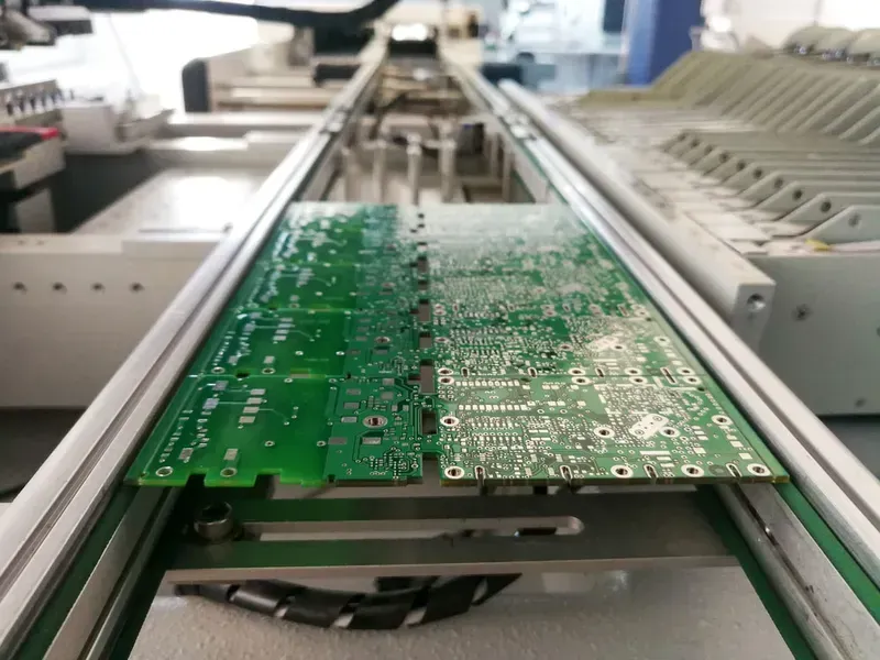
PCB Manufacturing Factory Production Line
Zero One Solution Limited stands at the forefront of providing comprehensive and cutting-edge PCB solutions specifically tailored for Home Energy Storage Systems (HESS). Our deep expertise, honed over years in the industry, allows us to address the complex requirements of HESS PCBs, ensuring optimal performance, safety, and longevity for these critical components. We leverage advanced manufacturing processes and a relentless commitment to quality, positioning ourselves as the ideal partner for rapid prototyping and mass production of highly reliable HESS PCB solutions.
Rapid Prototyping Excellence Our strength in rapid prototyping allows HESS innovators to quickly validate designs and accelerate their product development cycles. This agility is crucial in the fast-evolving energy storage market, enabling faster time-to-market and iterative improvements based on real-world testing. We understand that speed without precision is futile, so our prototypes mirror the quality of final production units.
Advanced Manufacturing Processes We employ state-of-the-art manufacturing technologies for HESS PCBs, including precision etching, multi-layer lamination, and advanced surface finishes. Our processes are optimized to handle high current densities, stringent thermal management requirements, and robust EMI/EMC compliance, all vital for the demanding environment of home energy storage.
Capability
Benefit for HESS PCBs
Technical Standard Adherence
High-Density Interconnect (HDI)
Enables compact, high-performance designs critical for space-constrained HESS units, improving signal integrity.
IPC-2226
Advanced Thermal Management Solutions
Utilizes specialized materials and designs (e.g., thick copper, thermal vias) to dissipate heat efficiently, enhancing reliability and lifespan of power components.
IPC-4101
Robust EMC/EMI Control
Implements precise shielding and grounding techniques to minimize electromagnetic interference, ensuring stable operation within residential environments.
IEC 61000 series
Comprehensive Quality Control
Rigorous testing protocols, including AOI, X-ray inspection, and functional testing, guarantee defect-free and high-performance PCBs.
IPC-A-600, ISO 9001:2015
Our commitment extends beyond manufacturing; we offer a collaborative partnership, providing expert guidance from initial design concepts to final product realization. This holistic approach ensures that every HESS PCB solution we deliver is not only technologically superior but also perfectly aligned with our clients' strategic objectives and the stringent demands of the home energy storage market.
Our One-Stop Service: From Design to Assembly
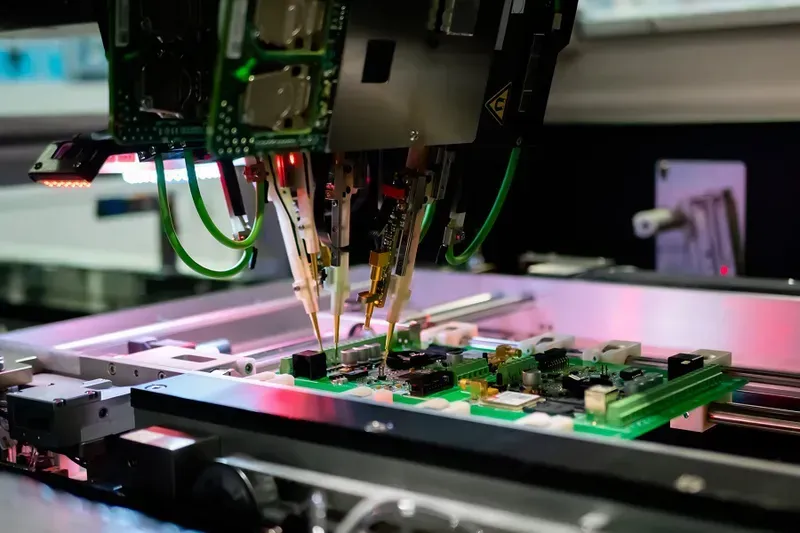
PCB Assembly and Testing
Zero One Solution Limited offers a truly integrated one-stop service for Home Energy Storage System (HESS) PCBs, streamlining the entire product development lifecycle from conceptual design to final assembly and rigorous testing. This comprehensive approach eliminates the complexities of managing multiple vendors, ensuring seamless communication, expedited timelines, and unparalleled quality control, all critical for the demanding performance and reliability requirements of HESS applications.
PCB Design & Optimization Our expert engineers collaborate closely with clients to optimize HESS PCB designs for performance, thermal management, EMC, and cost-effectiveness, leveraging advanced simulation tools and deep industry knowledge to meet specific power and safety standards. This includes material selection for optimal thermal conductivity and electrical properties, crucial for high-power HESS environments.
Rapid Prototyping Specializing in rapid prototyping, we accelerate your R&D cycles by quickly producing high-precision PCB prototypes. This allows for rapid iteration and validation of designs, significantly reducing time-to-market for innovative HESS solutions. Our agility in prototyping is a cornerstone of our value proposition.
Advanced PCB Manufacturing Utilizing state-of-the-art facilities and stringent quality control protocols, we manufacture HESS PCBs with precision and consistency. Our capabilities include handling complex multi-layer boards, high-current traces, and specialized materials required for robust and efficient energy storage systems. Every board undergoes strict inline inspections to maintain peak quality.
Component Sourcing & Procurement Leveraging our global supply chain network, we efficiently source high-quality, authentic electronic components for HESS PCBs. Our established relationships with leading suppliers ensure competitive pricing, timely delivery, and the authenticity of all parts, mitigating supply chain risks common in the electronics industry.
Automated PCBA & Manual Assembly We employ advanced SMT (Surface Mount Technology) and THT (Through-Hole Technology) processes for precise and reliable PCB assembly. For specialized HESS applications, our skilled technicians perform meticulous manual assembly where intricate connections or unique component placements are required, ensuring superior build quality.
Rigorous Testing & Quality Assurance Every HESS PCB and PCBA undergoes comprehensive testing, including Automated Optical Inspection (AOI), X-ray inspection for hidden defects, In-Circuit Testing (ICT), and Functional Testing (FCT) tailored to HESS operational parameters. This exhaustive testing regimen guarantees the highest levels of reliability, safety, and performance for critical energy storage applications.
Advantages of Partnering with Zero One Solution Limited for HESS PCBs
Partnering with Zero One Solution Limited for your Home Energy Storage System (HESS) PCB needs offers a transformative advantage in a rapidly evolving market. Our specialized expertise, rapid prototyping capabilities, and integrated one-stop service model translate directly into significant benefits for our clients, accelerating their product development cycles, optimizing costs, and ensuring the highest quality and reliability for their energy storage solutions. We are committed to empowering innovators to bring advanced HESS products to market efficiently and effectively.
Accelerated Time-to-Market In the competitive HESS market, speed is paramount. Zero One Solution Limited's rapid prototyping and streamlined manufacturing processes significantly reduce lead times from design to finished PCB. Our agility allows clients to iterate quickly, test concepts, and get their products to market faster, gaining a crucial competitive edge. This is achieved through optimized material procurement, efficient production lines, and an experienced engineering team capable of rapid design validation.
Unparalleled Cost-Efficiency Beyond competitive pricing, our one-stop service model eliminates the complexities and costs associated with managing multiple vendors for design, manufacturing, and assembly. This integrated approach reduces overheads, minimizes logistical delays, and optimizes the entire production lifecycle, leading to substantial overall cost savings without compromising on quality. Our scale and strategic location in Shenzhen further enhance cost efficiencies in the global supply chain.
Access to Cutting-Edge Technology We continuously invest in advanced PCB manufacturing technologies and materials, ensuring our clients benefit from the latest innovations relevant to high-power, high-reliability HESS applications. From advanced substrate materials to precise impedance control and superior thermal management solutions, we provide access to state-of-the-art capabilities that enhance system performance and longevity.
Expert Technical Support and Collaborative Partnership Our team of veteran engineers, with decades of experience in PCB design and manufacturing, offers unparalleled technical support throughout the entire project lifecycle. We act as a true partner, providing expert guidance from initial concept and material selection to design optimization, DFM (Design for Manufacturability) analysis, and rigorous testing, ensuring that every HESS PCB solution meets the highest standards of performance and safety.
Rigorous Quality Assurance and Reliability Quality is at the core of our operations. Zero One Solution Limited adheres to stringent quality control protocols and industry standards (e.g., IPC, ISO) at every stage, from material inspection to final functional testing. This meticulous approach guarantees the reliability, durability, and safety of HESS PCBs, which are critical for long-term energy storage applications. Our commitment to excellence minimizes potential failures and maximizes product lifespan.
Future Trends in Home Energy Storage PCB Technology
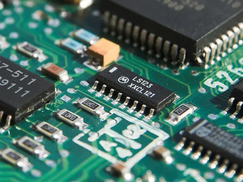
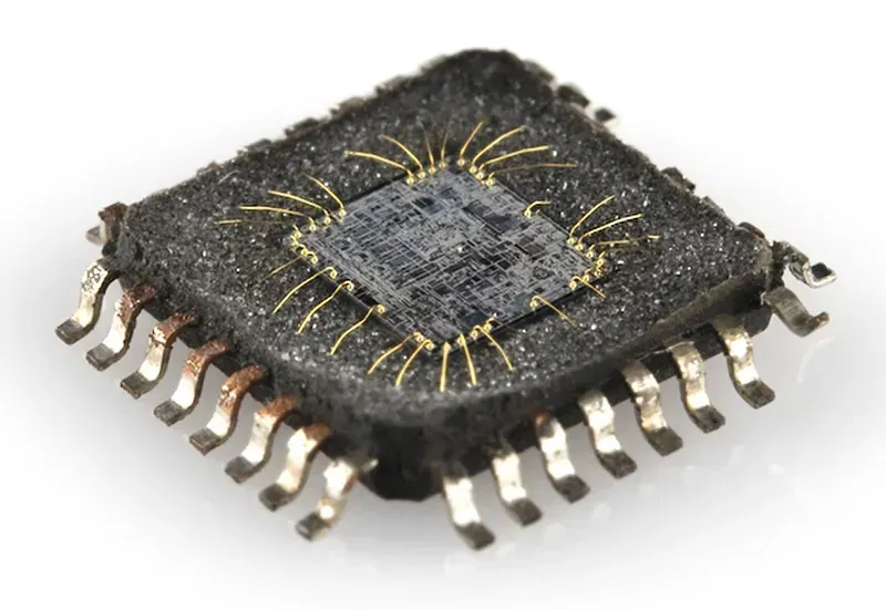
Integrated Circuit Chip
The evolution of Home Energy Storage Systems (HESS) is intrinsically linked to advancements in Printed Circuit Board (PCB) technology. As the demand for more efficient, compact, and reliable energy storage solutions grows, the PCBs at their core must adapt. Future trends in HESS PCB technology are converging on enhanced integration, superior thermal management, and a definitive shift towards sustainable manufacturing, driving the next generation of resilient and high-performing systems.
Enhanced Integration and Miniaturization Future HESS PCBs will feature higher levels of integration, combining multiple functions onto a single board to reduce system size, weight, and complexity. This includes integrating power electronics, control circuits, and communication modules, leading to more compact and efficient designs. Advanced packaging techniques like System-in-Package (SiP) and heterogeneous integration will become more prevalent, allowing for higher component density and shorter signal paths, which in turn improve performance and reduce parasitic effects. This trend is crucial for creating aesthetically pleasing and space-efficient home energy solutions. For instance, the integration of GaN and SiC power devices directly onto PCB substrates is set to revolutionize inverter and charger designs by enabling higher switching frequencies and efficiencies in smaller footprints, as evidenced by recent breakthroughs in wide-bandgap semiconductor integration.
Advanced Thermal Management Solutions As HESS become more powerful and compact, managing heat dissipation efficiently becomes paramount. Future PCBs will incorporate advanced thermal management features directly into their design and materials. This includes the widespread adoption of metal-core PCBs (MCPCBs), thermal vias, embedded heat sinks, and novel substrate materials with higher thermal conductivity. Techniques like liquid cooling integration at the board level and phase-change materials will also gain traction, ensuring optimal operating temperatures for sensitive components like power converters and battery management systems. Effective thermal management extends the lifespan of components, enhances system reliability, and prevents performance degradation, critical for long-term energy storage applications. According to a study by MarketsandMarkets, the thermal management solutions market is projected to grow significantly, driven by demand from power electronics, including those in renewable energy systems.
Sustainable and Eco-Friendly Manufacturing The push for sustainability extends to PCB manufacturing for HESS. Future trends will see a greater emphasis on using eco-friendly materials, reducing waste, and minimizing the environmental footprint throughout the production lifecycle. This includes the development and adoption of halogen-free laminates, lead-free solders, and bio-based resins. Furthermore, processes like additive manufacturing (3D printing of PCBs) offer the potential for reduced material waste and more localized production. Recycling and end-of-life considerations for PCBs will also become more standardized, aligning with circular economy principles. This commitment to sustainability not only addresses environmental concerns but also resonates with the ethos of renewable energy systems themselves, enhancing the overall value proposition of HESS.
Frequently Asked Questions about Home Energy Storage System PCBs
What are the primary design considerations for Home Energy Storage System (HESS) PCBs? The core design considerations for HESS PCBs revolve around high current handling, efficient thermal management, electromagnetic compatibility (EMC), and long-term reliability. Due to the high power requirements, PCBs must accommodate thick copper traces and robust power planes to minimize resistance and heat generation. Effective thermal dissipation, often through thermal vias and specialized materials, is critical to prevent overheating and ensure component longevity. EMC is vital to prevent interference with other electronic systems and ensure stable operation. Furthermore, the PCB must withstand environmental stressors, demanding robust material selection and meticulous layout for extended operational life.
Which materials are best suited for HESS PCBs? For Home Energy Storage System PCBs, materials are chosen for their electrical performance, thermal conductivity, and mechanical robustness. High-Tg (glass transition temperature) laminates like FR-4 derivatives or specialized ceramic-filled hydrocarbon materials are preferred for their stability at elevated temperatures. Copper thickness is crucial, often ranging from 2oz to 6oz or even higher in power sections, to manage high currents and dissipate heat effectively. Additionally, advanced dielectric materials with low loss tangents are used in high-frequency sections to ensure signal integrity and efficiency.
How are HESS PCBs tested to ensure reliability and safety? Testing for HESS PCBs is rigorous and multi-faceted, encompassing electrical, thermal, and environmental validations. Essential tests include In-Circuit Testing (ICT) and Functional Testing (FCT) to verify component placement and circuit operation. High-pot (dielectric strength) testing ensures insulation integrity under high voltage. Thermal cycling and accelerated aging tests simulate long-term operational stresses to assess reliability. Vibration and shock tests confirm mechanical robustness, while electromagnetic interference (EMI) and electromagnetic susceptibility (EMS) tests ensure compliance with EMC standards, crucial for safe and stable operation in a home environment.
What role does the Battery Management System (BMS) PCB play in HESS? The Battery Management System (BMS) PCB is the brain of a Home Energy Storage System, acting as a critical safeguard and optimizer for the battery pack. Its primary functions include precise cell voltage monitoring, current regulation during charge and discharge cycles, temperature management to prevent thermal runaway, and cell balancing to maximize battery lifespan and capacity utilization. The BMS PCB also implements safety features such as overcharge, over-discharge, over-current, and short-circuit protection, communicating the battery's state of charge and health to the main control unit, thereby ensuring the system's overall safety, efficiency, and longevity.
What are common failure points in HESS PCBs and how can they be mitigated? Common failure points in HESS PCBs often stem from inadequate thermal management, high current density issues, and environmental degradation. Overheating components due to insufficient heat dissipation can lead to premature failure. High current densities in narrow traces can cause localized hotspots and trace erosion. Environmental factors like humidity and temperature fluctuations can degrade materials over time. Mitigation strategies include optimizing PCB layout for efficient heat dissipation (e.g., wider traces, thermal vias, heat sinks), using robust materials with high thermal conductivity, incorporating conformal coatings for environmental protection, and implementing rigorous testing protocols to identify weaknesses before deployment. Proper design for manufacturability (DFM) and design for testability (DFT) also play crucial roles in preventing failures.
The future of home energy is undeniably linked to the advancement of reliable and efficient energy storage systems, and at the core of this evolution are robust and intelligently designed PCBs. Zero One Solution Limited stands as your premier partner, offering unparalleled expertise in PCB design, manufacturing, and assembly specifically tailored for Home Energy Storage Systems. Our commitment to rapid prototyping and one-stop service ensures that your innovations move from concept to market with exceptional speed and quality. Headquartered in Shenzhen and with a strategic branch in Dubai, we leverage a global supply chain to deliver solutions that meet the highest standards of performance and reliability. Don't let PCB complexities hinder your progress; contact Zero One Solution Limited today to discuss how our specialized PCB solutions can power your next generation of Home Energy Storage Systems.