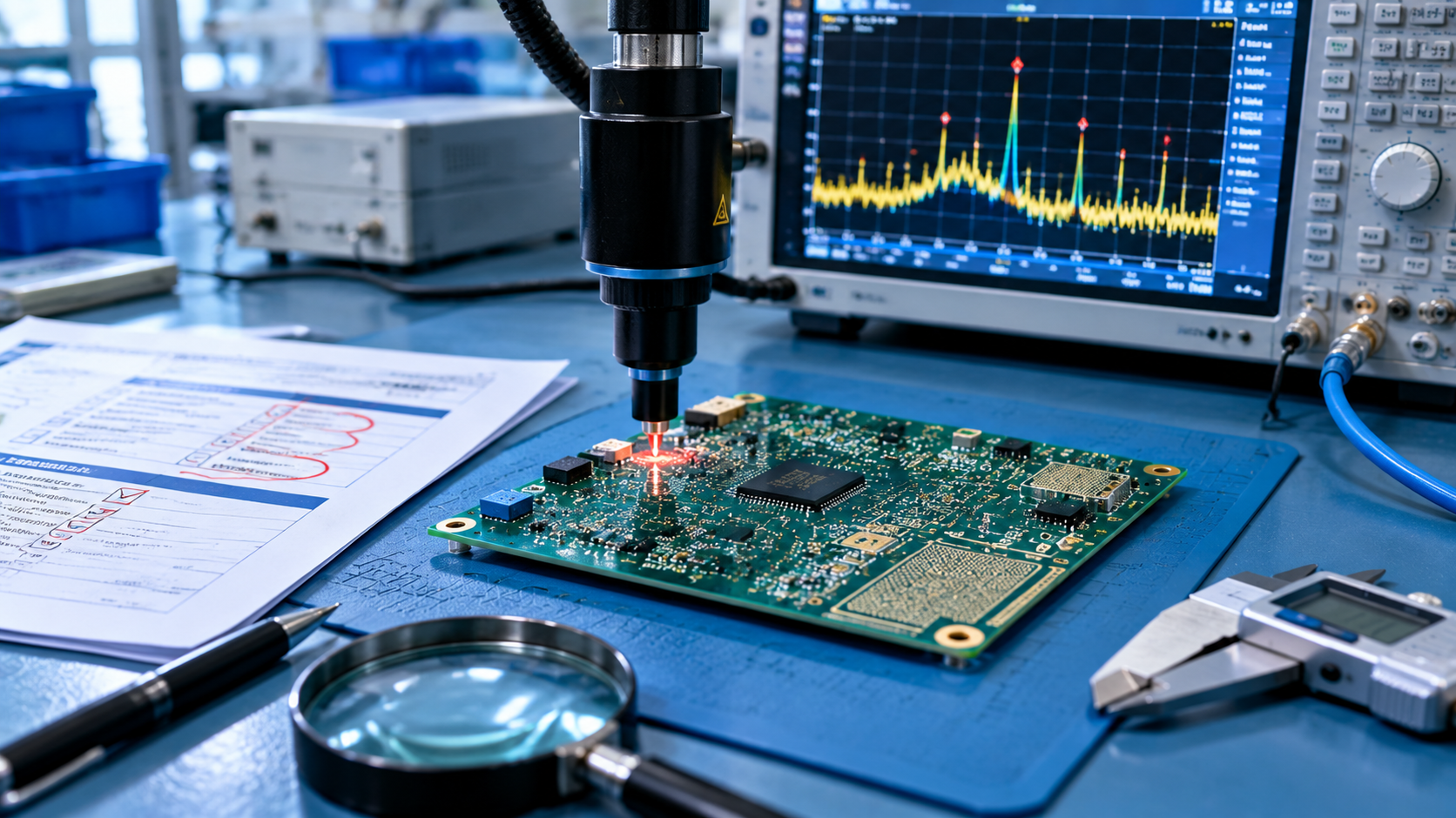
All electronic circuit boards exist to enable or enhance the flow of electricity to achieve specific performance goals. Current flows along closed paths, generating a magnetic field that extends outward and perpendicular to the current direction. When this field is near electronic components or signal paths, electromagnetic interference (EMI) occurs.
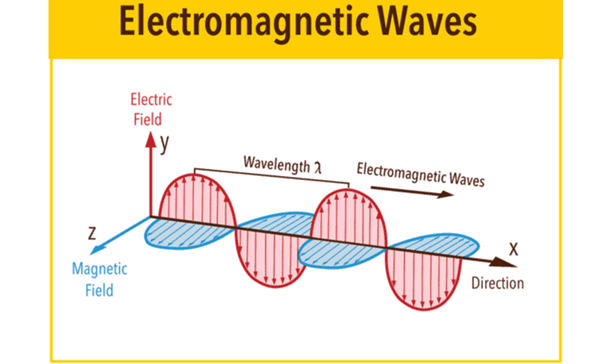
For many PCBA designs, controlling EMI is a primary concern — especially for high-speed circuit boards. For boards with radiating components, a common approach is EMI filter design. While filters are effective, PCB designers should also master additional PCB design methods that are essential tools for reducing EMI, often requiring flexible application.
Most PCBAs are not the only electronic or electrical device in a product. Therefore, before diving into board-level EMI issues, it's best to first understand EMI from a macro or system-level perspective.
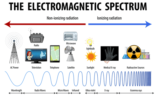
Just as electromagnetic energy radiates from individual components, conductors, or traces, the circuit board itself can release electromagnetic waves into the surrounding environment. If a Gaussian meter is placed near the PCB, related values can be measured. When multiple circuit boards are in close proximity, achieving electromagnetic compatibility (EMC) becomes especially important.
EMC aims to ensure minimal EMI between devices, thereby ensuring normal operation of the equipment. While EMI cannot be completely eliminated, EMC can be achieved. EMI typically refers to interference on a single PCBA; reducing EMI helps improve the EMC level of the surrounding environment.
| Source | Description |
|---|---|
| Components | Electronic components, especially processors, FPGAs, amplifiers, transmitters, and antennas — high-power devices are often significant EMI sources. Switching components can also generate electromagnetic interference that damages the entire system. |
| Signals and Traces | EMI can propagate along traces and can also be generated at pins and connector points. Improper differential pair routing can cause signal attenuation and reflection, affecting signal integrity and even causing abnormal circuit behavior. Additionally, stray capacitance can cause unnecessary coupling between signal paths and ground planes. |
| External Sources | If the circuit board is too close to a radiation source (such as other circuit boards or components), EMI can be introduced. Vibration or movement of surrounding equipment or devices can also generate harmonics. |
| Measure | Description |
|---|---|
| Select Low-Power Components | Choose low-power components to reduce EMI. High-power components typically generate more EMI; low-power components can maintain functionality while reducing interference. |
| Isolate Different Component Types | Group components handling similar signals together. Place digital components close to each other and away from analog components. |
| Use PCB Shielding | Use PCB guard rings, Faraday cages, or similar shielding around components or sub-circuits to effectively reduce EMI and prevent radiation from affecting the surrounding environment. |
| Apply Thermal Management | Use heatsinks and thermal vias to effectively manage heat generated by components and minimize EMI. |
During PCB layout, spacing is one of the most important considerations, including ensuring sufficient clearance and creepage distance between conductive elements.
For multilayer boards, the stacking order and distance between conductive planes and ground planes are also critical.
| Measure | Description |
|---|---|
| Leave Sufficient Spacing Between Signal Traces | To effectively reduce EMI between traces, the primary factor is spacing or clearance. Follow the recommendations of IPC-based rule managers. |
| Ensure Decoupling and Bypass Capacitors Are Grounded | Stray capacitance is difficult to eliminate completely, but placing capacitors as close as possible to pins and grounding them effectively reduces the impact. |
| Adopt Good EMI Filter Design | Most designs, especially those using digital signals, contain switching components that can cause signal distortion. In these cases, using filters is the best measure to improve signal fidelity. |
Minimizing external EMI is critical for signal integrity and circuit operation on the board, and helps the EMC of the PCBA installation environment.
Measures to reduce EMI from external sources:
Use shielding devices: Shielding devices are typically used to cover specific components or sub-circuits. Unlike guard rings, shielding devices are usually made of insulating material and are placed on top of components or completely enclose them.
Use enclosures: Enclosures are often viewed as safety devices. However, they can also effectively protect circuit boards from debris and external EMI.
PCB layout (including stackup structure) helps ensure good signal integrity and reduce EMI. However, any PCB design guideline aimed at reducing EMI is incomplete without addressing external EMI suppression measures.
Reducing EMI and optimizing EMC requires a combination of strategies:
| Area | Key Measures |
|---|---|
| Components | Low-power selection, isolation, shielding, thermal management |
| Signals & Planes | Trace spacing, decoupling capacitor grounding, EMI filter design |
| External Sources | Shielding devices, enclosures |
Need EMI/EMC Design or Manufacturing Support?
AnyPCBA's engineering team focuses on EMI reduction, EMC optimization, and signal integrity during design reviews. Whether you're working on high-speed digital designs or mixed-signal boards, we provide DFM/DFA design reviews to identify potential EMI risks before fabrication.
Our manufacturing capabilities cover 2-64 layers, including HDI, rigid-flex, and high-frequency hybrid processes.
Contact us to discuss your project →




