
Only when a PCB design fully captures all the information required for successful assembly is the design truly complete. Even after routing is finished, inspections and reviews are still needed to ensure the PCB can be assembled correctly. For items that cannot be defined by design rules, manual review by the designer is mandatory.
This guide covers the key elements designers should review before releasing a design for prototype or mass production. Because these checks require a deep understanding of design intent, DRC alone often cannot cover them all.
Silkscreen on the top and bottom layers contains critical information for assembly, testing, debugging, and traceability. Check for the following errors:
Check for overlapping or too-close reference designators. If relevant design rules are not applied, DRC will not report these errors — manual inspection of the silkscreen layer is required.
Ensure reference designators do not fall on pads or open vias. Spacing rules may also fail to catch these issues, depending on how the rules are defined.
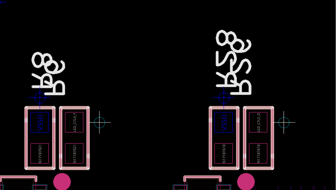
Ensure part numbers are placed in easily readable areas. Apply the same check to company logos, CE/FCC certification marks, and ESD protection symbols.
Set an appropriate font size for reference designators so they are clearly legible without optical aids.
Check whether component footprints include polarity markings and pin-1 indicators. Ensure the outline is not positioned underneath the component body.
Add polarity markings to power input terminals, indicating voltage and current ratings.
This checklist can be performed visually or using the DRC engine in PCB design software.
During routing, it's easy to place vias that seem reasonable at the time — but this leads to inconsistent hole sizes throughout the design. Some hole sizes may not conform to standard drill sizes, forcing manufacturers to adjust and adapt to their existing tooling.
It is essential to comprehensively review vias and set them to uniform hole sizes. Avoid using different drill sizes where possible, and ensure drill bits are standard sizes.
Another key parameter for hole sizes is tolerance. Any tolerance range can be specified, but specific values must be clearly documented. The issue is that manufacturers may not be able to achieve the specified tolerance targets. Drill tolerances (whether for drill size or finished hole size) are recommended at ±3 mil (±0.075mm).
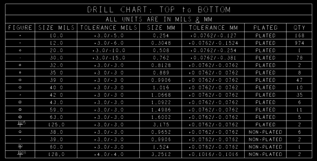
Other areas also have tolerance requirements — particularly in manufacturing notes, which define tolerances for layer stackup, trace width, impedance targets, and board dimensions. If not clearly specified, the fabricator will set their own values, which may not meet application requirements. Always clearly state manufacturing requirements.
If mechanical requirements were defined early in the design, you already have a mechanical checklist before sending the board to manufacturing and assembly. Even if the PCB design is complete, the positions of connectors and critical mechanical components must still be verified.
Example: Is the position of this hole near the board edge correct? Always measure the hole position coordinates.
If certain mechanical checks can be skipped, ensure critical mechanical components are locked in the PCB design. Mounting holes, connectors, fiducial marks, and major components (such as large processors) should be locked in position early and should not be moved unless absolutely necessary.
Even after executing the full design check process, there may still be DRC errors that need to be resolved. Sometimes, after performing checks and implementing fixes, new DRC violations can be generated. Therefore, before generating output files, run DRC again as a final check to ensure all violations have been resolved.
Before finalizing the design and preparing output files for manufacturing, all violations must be completely resolved.
Before releasing a PCB design for manufacturing, complete these four critical checks:
| Check Area | Key Actions |
|---|---|
| Silkscreen | Check overlapping designators, readability, polarity markings, pin-1 indicators |
| Hole Sizes & Tolerances | Standardize via sizes, document tolerances (±3 mil recommended), specify manufacturing requirements |
| Mechanical | Verify connector positions, measure hole coordinates, lock critical components |
| DRC | Run final DRC after all fixes, resolve all violations before output |
Need PCB Design Review or Manufacturing Support?
AnyPCBA's engineering team provides DFM/DFA design reviews to help you identify potential issues in silkscreen, drill sizes, mechanical alignment, and DRC before fabrication. Our manufacturing capabilities cover 2-64 layers, including HDI, rigid-flex, and high-frequency hybrid processes.
Contact us to discuss your project →




