
In the modern high-density data center, even the smallest component failure can trigger catastrophic downtime. At the heart of your power distribution unit (PDU) lies the PCB—a critical piece of hardware that often goes overlooked until a power surge or thermal event occurs. This guide provides an authoritative roadmap for selecting PDU PCBs that balance raw power capacity with uncompromising safety and reliability.
Understanding the Role of the PDU PCB in Power Distribution
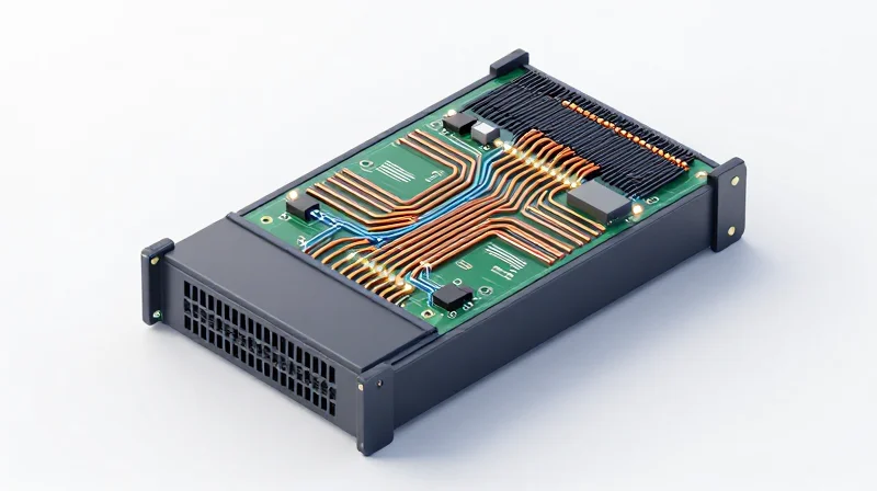
In a Power Distribution Unit (PDU), the Printed Circuit Board (PCB) is far more than a simple mounting substrate; it acts as the primary busbar system that facilitates high-current delivery from the input source to individual outlet modules. Because modern data centers demand increasingly higher power densities, the PCB often becomes the limiting factor in power path integrity. If the board's copper traces or layer stack-up are insufficient, they become points of high electrical resistance, resulting in excessive heat generation, voltage drops, and potential infrastructure failure.
The PCB as a Thermal and Electrical Bottleneck
The fundamental challenge in high-current PCB design is managing the trade-off between current-carrying capacity and thermal management. As current flows through conductive copper paths, Joule heating occurs—a phenomenon governed by the resistance of the trace material. In server PDUs, this requires substantial copper weight and strategically placed thermal vias to dissipate heat across the board surface and into the chassis.
| Parameter | Effect on Reliability | Performance Constraint |
|---|---|---|
| Copper Weight | Higher weight reduces resistance and heat. | Manufacturing limitations on fine-pitch components. |
| Layer Count | Distributes current across multiple planes. | Increased complexity and signal integrity risks. |
| Trace Geometry | Width determines peak ampacity. | Limited space within dense PDU form factors. |
Key Engineering Considerations for PDU PCBs
- How does copper thickness affect power delivery?
Increased copper thickness, typically measured in ounces (oz) per square foot, directly lowers the DC resistance of the traces. Lower resistance equates to lower power loss as heat, allowing the PDU to operate safely at higher amperage levels without damaging board integrity. - What role do thermal vias play in PCB safety?
Thermal vias act as conduits to transfer heat from high-current layers to the PCB’s outer surfaces or internal heat-sinking planes. Without adequate via density, local hot spots can degrade the dielectric material, leading to delamination or electrical arcing. - Why is the dielectric material critical for PDUs?
High-current boards generate intense localized heat. Choosing a substrate with a high Glass Transition Temperature (Tg) is essential to ensure that the PCB material remains structurally sound and does not soften or deform under continuous high-load operation.
Current-Carrying Capacity and Copper Thickness
The Physics of Current-Carrying Capacity
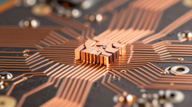
The current-carrying capacity of a PCB trace is defined by its ability to conduct electricity without exceeding its maximum rated operating temperature. This is governed by the IPC-2221 standard, which correlates cross-sectional area—the product of trace width and copper thickness—with temperature rise. In PDU applications, where continuous high current is the norm, insufficient copper cross-section leads to ohmic heating, increasing board temperature, degrading laminate materials like FR-4, and potentially causing long-term failure.
Copper Weight and Thermal Performance
Copper thickness is standardly measured in ounces (oz) per square foot. Increasing copper weight reduces electrical resistance, which directly lowers heat generation at a constant current. While increasing trace width is an effective way to handle more current, it increases the PCB footprint. Increasing copper thickness allows for higher current density within the same trace width, facilitating more compact designs.
| Copper Weight (oz) | Thickness (mm) | Application Focus | Heat Dissipation |
|---|---|---|---|
| 1 oz | 0.035 mm | Logic signals, low power | High thermal resistance |
| 2 oz | 0.070 mm | Intermediate power distribution | Moderate thermal resistance |
| 3+ oz | 0.105+ mm | High-current PDU busbars | Low thermal resistance |
Frequently Asked Questions
- Why is trace width alone not sufficient for high-current design?
Trace width must be balanced with copper thickness to achieve the required cross-sectional area. Relying solely on width leads to inefficient space usage, whereas increasing copper thickness optimizes current density. - How does PCB temperature affect PDU reliability?
Excessive heat causes thermal stress on PCB materials and solder joints. Prolonged operation at elevated temperatures leads to delamination, oxidation of copper, and eventual catastrophic failure of the power distribution infrastructure. - Is thicker copper always better for high-current PDUs?
While thicker copper improves electrical and thermal performance, it increases manufacturing complexity, costs, and can complicate fine-pitch component assembly; it must be balanced against design requirements.
Advanced Thermal Management Strategies
Advanced Thermal Management Strategies
Reliable high-current power distribution requires more than just thick copper; it demands a holistic thermal ecosystem. By integrating high-Tg base materials with enhanced via stitching and conductive heatsinking, engineers can effectively mitigate hotspot formation that leads to dielectric degradation.
High-Tg Materials and Thermal Stability
Standard FR-4 materials often fail under continuous high-current thermal cycling. Selecting materials with a high Glass Transition Temperature (Tg) is essential to maintain structural integrity and prevent delamination. Below is a comparison of common PCB material classes for high-current applications:
| Material Type | Typical Tg (°C) | Thermal Reliability | Best Use Case |
|---|---|---|---|
| Standard FR-4 | 130-140 | Low | Low-current control logic |
| High-Tg FR-4 | 170-180 | High | Main power distribution buses |
| Ceramic-filled Polyimide | >250 | Extreme | High-temp mission-critical systems |
Optimizing Heat Dissipation Channels
- How do thermal vias contribute to PCB longevity?
Thermal vias act as heat pipes, transferring thermal energy from the inner copper layers to the outer surfaces or heat-spreading planes, significantly reducing localized board temperatures. - Are there specific guidelines for via array density?
Vias should be placed as close as possible to the high-current components with a pitch optimized to prevent excessive resin starvation, typically maintaining a minimum of 0.5mm between drill centers. - What role do external heatsinks play on PDU PCBs?
For high-current segments, direct mounting of copper-based heatsinks to the PCB surface—via thermal interface material (TIM)—provides a secondary path for heat dissipation, essential for sustained high-amperage operation.
Material Selection: Laminates and Substrates
Evaluating Laminate Performance for High-Current PDUs
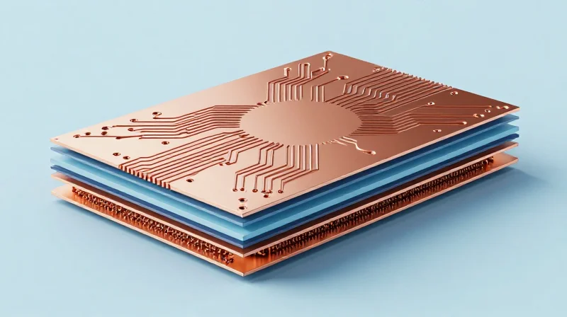
Standard FR-4 is often insufficient for high-current server PDUs due to its lower glass transition temperature (Tg) and limited thermal stability, which can lead to delamination or trace separation under repeated thermal cycling. In high-power infrastructure, engineers must prioritize laminates that offer superior thermal management, dimensional stability, and high dielectric strength to prevent catastrophic board failure.
Material Comparison Matrix
| Material Type | Typical Tg (°C) | Thermal Reliability | Best Use Case |
|---|---|---|---|
| Standard FR-4 | 130-140 | Low | Low-power consumer electronics |
| High-Tg FR-4 | 170-180 | Moderate | General server backplanes |
| Polyimide/Specialty | 250+ | High | High-current industrial/data center PDUs |
Selecting the Right Substrate: Common Considerations
- Why is the Glass Transition Temperature (Tg) so critical?
The Tg indicates the temperature at which the laminate transitions from a rigid, glass-like state to a rubbery state. Operating near or above this threshold leads to expansion, which stresses copper traces and via barrels, eventually causing electrical open circuits. - How does Coefficient of Thermal Expansion (CTE) impact reliability?
Materials with low CTE, specifically in the Z-axis, are essential to match the thermal expansion of copper. Mismatched CTEs between the substrate and copper induce mechanical fatigue on plated through-holes during power-cycling events. - Is metal-core PCB (MCPCB) a viable alternative for PDUs?
Yes, for extreme current densities, integrating an aluminum or copper core provides superior thermal conductivity. However, it requires different manufacturing processes and considerations for dielectric breakdown between the core and conducting layers.
For reliable PDU design, prioritize high-Tg (>170°C) substrates combined with low-loss, thermally stable resin systems. These materials ensure the board maintains mechanical rigidity despite the significant heat generated by high-amperage current flow.
Adherence to International Electrical Safety Standards
Essential Compliance Standards for PDU PCBs
For data center infrastructure, safety is non-negotiable. PDU PCBs must be designed and manufactured in strict accordance with global standards to mitigate risks of electrical shorts, thermal runaway, and fire. Manufacturers must prioritize UL, IEC, and IPC compliance to ensure the hardware can withstand the demanding electrical loads of modern high-density server racks.
| Standard Body | Primary Focus | Significance for PDUs |
|---|---|---|
| UL (Underwriters Laboratories) | Safety and Flammability | UL 796 certifies PCB safety, while UL 94-V0 mandates strict flame retardancy. |
| IEC (International Electrotechnical Commission) | Performance and Clearance | IEC 60950-1 and IEC 62368-1 define critical creepage and clearance distances. |
| IPC (Association Connecting Electronics Industries) | Reliability and Fabrication | IPC-2152 provides the standard for determining current-carrying capacity. |
Critical Safety Requirements Explained
- Creepage and Clearance (IEC 62368-1)
These standards dictate the shortest path between conductive parts. Adequate spacing is essential to prevent electrical arcing and tracking, especially in high-voltage AC environments. - Flammability Rating (UL 94-V0)
Materials used in PDU PCBs must carry a V0 rating, meaning the material will cease burning within 10 seconds on a vertical specimen, preventing the spread of fire. - Current Capacity Validation (IPC-2152)
Moving beyond legacy standards like IPC-2221, IPC-2152 uses physics-based models to calculate temperature rise, ensuring the PCB does not exceed its maximum operating temperature under peak load.
Ensuring Long-Term Compliance
Beyond initial certification, reliability is maintained through rigorous testing cycles, including High-Pot (high-potential) dielectric withstand testing and thermal cycling. Selecting a PCB manufacturer that maintains traceable UL 'Yellow Cards' for their laminates ensures that the raw materials—and the final assembly—consistently meet the stringent safety thresholds required for mission-critical data center power infrastructure.
Optimizing PCB Layout for Power Integrity
Minimizing Impedance and Voltage Drops
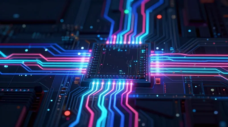
In high-current PDU applications, the PCB layout must prioritize low-impedance power distribution networks (PDN). Excessive DC resistance leads to localized heating and significant voltage drops, which can degrade server performance. Designers should utilize wide, heavy copper traces and maximize the copper weight—typically 2 oz to 4 oz—to keep current density within safe limits.
Strategies for Effective Power Delivery
- Trace Geometry
Utilize short, wide paths to connect components, reducing the overall loop area and minimizing parasitic inductance. - Layer Stack-up
Use dedicated internal power and ground planes to provide a continuous return path, which significantly lowers impedance and manages return current flow. - Component Placement
Place decoupling capacitors as close as possible to the power input pins to provide instantaneous current and filter high-frequency noise.
EMI Mitigation and Signal Integrity
High-current switching events in server PDUs create electromagnetic interference (EMI) that can disrupt sensitive logic signals. Implementing robust layout practices prevents these transient fields from coupling into data traces or affecting neighboring equipment.
| Layout Technique | Primary Benefit | Implementation Tip |
|---|---|---|
| Plane-to-Plane Coupling | Reduced Inductance | Place power/ground planes on adjacent layers. |
| Stitching Vias | EMI Shielding | Use stitching vias around board edges to create a Faraday cage. |
| Split Plane Management | Noise Isolation | Avoid running signal traces over gaps in the reference plane. |
Frequently Asked Questions
- How does copper thickness affect PDN performance?
Thicker copper reduces DC resistance and thermal stress, allowing for higher current handling without exceeding temperature rise limits. - Why is minimizing loop area important?
Minimizing loop area directly reduces radiated emissions and parasitic inductance, both of which are critical for maintaining clean power in dense data centers.
Reliability Testing and Quality Assurance Protocols
Validating PCB Longevity Through Rigorous Testing
Reliability in high-current power distribution units is not an assumption but a verified metric achieved through aggressive environmental stress screening. Because these PCBs handle sustained high amperages, they are susceptible to thermal fatigue and micro-fracturing at interconnect points; therefore, manufacturers must implement testing cycles that simulate years of operation within accelerated timeframes.
Primary Validation Methodologies
- Thermal Shock Testing
Boards undergo rapid temperature transitions between -40°C and +125°C to stress solder joints and via barrels, ensuring the coefficient of thermal expansion (CTE) mismatch between the copper and substrate does not lead to delamination. - Power Cycling Endurance
Units are subjected to continuous high-current loads with intermittent power-on/off cycles to evaluate the mechanical stability of copper traces under extreme Joule heating conditions. - Cross-Sectional Analysis
Destructive physical analysis is performed on post-test samples to inspect for barrel cracking, plating voids, and internal layer separation at the microscopic level.
Quality Assurance Metric Comparison
| Testing Protocol | Primary Failure Mode Detected | Key Indicator of Quality |
|---|---|---|
| Thermal Shock | Interconnect fracture | Consistent CTE alignment |
| High-Current Cycling | Trace delamination | Stable thermal dissipation |
| Cross-Sectioning | Plating thickness variance | Uniform copper coverage |
Establishing QA Standards for Procurement
When sourcing PDU PCBs, ensure that the manufacturer provides a comprehensive 'Certificate of Conformance' alongside documented test reports. Adherence to IPC-6012 Class 3 standards is non-negotiable for high-reliability infrastructure, as this dictates stringent requirements for hole wall copper thickness and surface finish integrity. By enforcing these QA protocols, data center operators can proactively mitigate the risk of catastrophic power failure and extended system downtime.
Future-Proofing Your Data Center Infrastructure
Designing for Scalability and Modular Upgrades
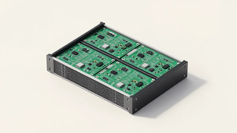
To prevent premature obsolescence, engineers must prioritize modularity in PDU PCB architectures. By utilizing busbar-integrated PCB designs or swappable daughter-card systems, operators can upgrade individual power rails or monitoring modules without replacing the entire power distribution assembly. This decoupled approach allows infrastructure to grow from standard 1U configurations to high-current multi-phase requirements as server rack power density inevitably increases.
Planning for Increased Thermal and Current Loads
Future-proofing is heavily dependent on specifying PCBs that exceed today's peak current requirements. By designing with wider copper cross-sections and higher thermal dissipation thresholds, you create a buffer for future hardware generations that may draw significantly more power.
| Strategy | Future-Proofing Benefit | Implementation Tip |
|---|---|---|
| Over-dimensioning Copper | Handles future power spikes | Use 4oz+ copper layers |
| Modular I/O Ports | Adapts to new connector standards | Design for swappable modules |
| Digital Twin Modeling | Predicts thermal degradation | Utilize FEA simulation tools |
Frequently Asked Questions
- How much overhead should be factored into PDU PCB current ratings?
A minimum of 20-30% overhead beyond your current peak load is recommended to ensure the PCB operates in a safe thermal zone during unexpected power surges or future hardware density increases. - Does modularity impact power integrity?
While modular connections introduce potential contact resistance, modern high-current connectors and redundant busbar designs effectively mitigate these risks, provided the layout maintains strict impedance control.
Selecting the right PDU PCB is not just a technical procurement task; it is an investment in your data center's long-term stability and operational safety. By prioritizing material quality, thermal design, and strict adherence to global safety standards, you mitigate the risk of catastrophic power failure. Ready to optimize your infrastructure? Contact our engineering team today for a consultation on your custom power distribution requirements.
