
In the rapidly evolving landscape of commercial space, the reliability of your satellite communication hardware is defined at the atomic level of your PCB. As signal frequencies push into the Ka and V bands, the margin for error in substrate selection vanishes. This guide breaks down the technical imperatives of choosing high-frequency materials that withstand the harsh realities of space while maintaining peak performance.
Understanding the Role of Dielectric Constant (Dk) Stability

The Critical Nature of Dk Stability
In satellite communication infrastructure, where signal wavelengths at Ka-band and beyond are extremely short, even minor fluctuations in the dielectric constant (Dk) can lead to catastrophic phase shifts. Dk stability defines how consistently a substrate maintains its electromagnetic properties across varying frequencies and operational temperatures. For high-performance satellite transceivers, selecting a material with a tight Dk tolerance is not merely an optimization; it is a fundamental requirement to ensure consistent signal propagation velocity and phase synchronization across the entire communication array.
Frequency and Thermal Dependency
Satellite equipment is often subject to extreme orbital temperature shifts and high-bandwidth requirements. Materials that exhibit high 'Dk versus temperature' coefficients will cause the circuit's electrical length to drift, leading to unintended phase noise. Furthermore, as frequency increases, Dk dispersion—where the Dk value changes relative to the operating frequency—can cause group delay distortion, degrading the quality of digital signals in sensitive transceivers.
| Parameter | Impact of Instability | Requirement for Satellite |
|---|---|---|
| Temperature Sensitivity | Phase shift and signal drift | Low TCDk (Near-zero ppm/°C) |
| Frequency Dispersion | Pulse broadening and data errors | Flat Dk curve from 10-100 GHz |
Frequently Asked Questions
- Why does Dk stability matter for phase-sensitive applications?
Phase velocity depends on the square root of Dk. If Dk fluctuates due to heat, the electrical phase changes, causing synchronization errors in phased-array antennas. - How do I evaluate a substrate's Dk performance?
Look for the material's TCDk (Temperature Coefficient of Dielectric Constant) rating on the datasheet and request broadband characterization data to identify dispersion across your target operating frequency range.
Minimizing Signal Loss: The Importance of Loss Tangent

In satellite communication, where signal power is limited and path loss is extreme, the dielectric material's loss tangent (also known as dissipation factor or Df) determines how much electromagnetic energy is converted into heat. As frequencies move into the Ka-band and beyond, even a marginal increase in the loss tangent can result in significant signal attenuation, drastically reducing the effective radiated power (EIRP) and G/T sensitivity of the satellite terminal.
The Impact of Loss Tangent on Link Performance
The loss tangent is a direct measure of the dielectric's inefficiency. A lower Df ensures that more power reaches the antenna, which is critical for maintaining reliable throughput in broadband satellite links. Engineers must prioritize substrates with extremely low loss profiles to mitigate the compound losses occurring within long transmission lines and complex feed networks.
| Material Grade | Typical Loss Tangent (Df) | Primary Application |
|---|---|---|
| Standard FR-4 | 0.020 | Low-frequency control logic |
| High-Frequency Epoxy | 0.004 | L-band/S-band transceivers |
| PTFE/Ceramic Filled | 0.001 - 0.002 | Ka-band/V-band Satellite Links |
Design Considerations and Frequently Asked Questions
- How does moisture absorption affect loss tangent?
Materials with high moisture absorption rates experience a sharp increase in loss tangent when exposed to humidity. Satellite infrastructure, often deployed in variable environments, requires materials with near-zero moisture absorption to prevent signal degradation over time. - Is Df constant across all frequencies?
No, loss tangent typically increases with frequency. Selecting a substrate requires evaluating the Df at the specific operating frequency of the satellite link, rather than relying on 1 MHz or 1 GHz data sheets. - Does copper surface roughness impact the total loss?
Yes. At high frequencies, the skin effect forces current to flow near the surface of the conductor. If the copper-dielectric interface is rough, the effective path length increases, compounding the losses inherent in the dielectric substrate.
To achieve superior signal integrity, designers should pair low-loss substrates with ultra-low-profile copper foils. This combination minimizes both dielectric heating and resistive losses, providing the robust performance necessary for reliable commercial satellite communication infrastructure.
Thermal Management and Coefficient of Thermal Expansion (CTE)
Thermal Management and Coefficient of Thermal Expansion (CTE)
In the vacuum of space, commercial satellites experience extreme thermal cycling as they transition between direct solar radiation and the deep cold of orbital shadows. For high-frequency PCB substrates, the Coefficient of Thermal Expansion (CTE)—specifically along the Z-axis—is the most critical metric for preventing structural failure. Mismatched expansion rates between the dielectric, copper traces, and plated through-holes (PTHs) create significant shear stress, which often manifests as micro-cracking or pad cratering during rapid temperature swings.
Mitigating Thermomechanical Stress
To ensure interconnect integrity, engineers must prioritize materials that offer a low Z-axis CTE, ideally matching that of copper (approximately 17 ppm/°C). Materials reinforced with woven glass cloth or ceramic fillers are typically preferred for high-frequency satellite applications, as they offer the mechanical rigidity necessary to constrain dielectric expansion. Failure to align these coefficients leads to increased parasitic impedance and potential signal path interruptions.
| Material Class | Typical Z-Axis CTE (ppm/°C) | Suitability for Satellite | Key Advantage |
|---|---|---|---|
| Standard FR-4 | 60-80 | Low | Cost-effective |
| Ceramic-filled PTFE | 25-40 | High | Thermal stability |
| Hydrocarbon Ceramic | 20-30 | Excellent | Low signal loss |
Thermal Management FAQ
- Why is the Z-axis CTE more critical than the X/Y axes?
Z-axis expansion drives the vertical strain on plated through-holes and vias; excessive movement causes mechanical fatigue, leading to barrel cracking and signal loss. - Does thermal conductivity of the substrate matter for high-frequency designs?
Yes, high-power satellite transceivers generate significant heat. Materials with higher thermal conductivity effectively spread heat away from active components, preventing localized dielectric degradation. - How does Tg (Glass Transition Temperature) influence satellite PCB selection?
A high Tg ensures the substrate remains in a stable, glassy state across the entire operating temperature range, preventing sudden changes in physical properties that could shift the PCB's resonant frequencies.
Adhering to IPC-6012 and Aerospace Standards
Navigating IPC-6012 Class 3/Space Requirements
The IPC-6012 specification for rigid printed circuit boards defines the qualification and performance requirements necessary for high-reliability electronics. For satellite infrastructure, compliance with IPC-6012 Class 3 (High Reliability) or the specific requirements for space applications (Class 3/Space) is mandatory. These standards mandate rigorous testing protocols, including microsection analysis, thermal shock cycling, and ionic contamination testing, to ensure the substrate can withstand the rigorous launch environment and subsequent thermal vacuum cycles in orbit.
Comparison of PCB Performance Standards
| Requirement | IPC-6012 Class 2 | IPC-6012 Class 3/Space |
|---|---|---|
| Target Reliability | General/Consumer | Space/Aerospace |
| Insulation Resistance | Standard | Enhanced/Strict |
| Plating Voids | Permitted within limits | Strictly prohibited |
| Microsectioning | Representative | Per-lot/Mandatory |
Quality Assurance and Regulatory Compliance
Beyond IPC-6012, aerospace-grade manufacturing requires strict adherence to AS9100 Quality Management Systems. This ensures total traceability of raw materials, from copper-clad laminate to final finish. Substrate selection must be vetted not only for RF performance but for material provenance, as material batch variance can lead to unpredictable dielectric consistency, potentially jeopardizing communication links across a constellation.
- Why is IPC-6012 Class 3/Space critical for satellites?
It sets the stringent criteria for plating thickness, material integrity, and void-free drilling, ensuring the PCB does not fail under the extreme mechanical stress of launch or the thermal cycling of space. - Does aerospace standard compliance impact RF performance?
Yes, through requirements for surface roughness control and copper adhesion testing, which ensure that high-frequency signal propagation remains stable over the mission lifespan. - How do we verify material conformity?
By requiring Certificate of Conformance (CoC) documentation and periodic testing of material samples to ensure they meet specified dielectric constants (Dk) and loss tangents (Df) as per the design requirements.
Material Selection: PTFE vs. Filled Hydrocarbon Ceramics
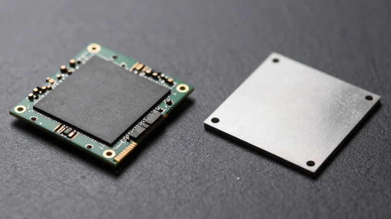
Material Performance and Structural Considerations
In the high-frequency environment of satellite communication infrastructure, the choice of substrate significantly influences both signal integrity and mechanical survivability. PTFE-based materials, renowned for their exceptionally low dielectric loss, are the industry standard for high-frequency performance but present challenges in structural stability. Conversely, filled hydrocarbon ceramic substrates offer improved rigidity and lower coefficient of thermal expansion (CTE) values, making them better suited for multi-layer high-density designs where thermal cycling is a persistent threat.
| Feature | PTFE-based Substrates | Filled Hydrocarbon Ceramics |
|---|---|---|
| Dielectric Loss (Df) | Extremely Low | Low/Moderate |
| Dimensional Stability | Low (Processing sensitive) | High |
| Thermal Conductivity | Moderate | Good |
| Ease of Fabrication | Difficult (Requires specialized handling) | Standard (FR-4 like processes) |
| Cost | Premium | Moderate |
Comparative Evaluation for Space-Grade Reliability
- Why is PTFE often preferred despite fabrication difficulties?
PTFE provides the lowest possible loss tangent, which is critical for maintaining link budgets in high-frequency satellite transponders where every decibel of signal strength is precious. - Do hydrocarbon ceramics meet space environmental requirements?
Yes, filled hydrocarbon ceramics offer superior mechanical integrity during launch-related vibration and temperature fluctuations, reducing the risk of via barrel cracking compared to legacy PTFE materials. - Which material is more cost-effective for mass-constellation deployment?
Filled hydrocarbon ceramics are typically more cost-effective as they align with standard high-speed multilayer PCB fabrication techniques, whereas PTFE necessitates specialized etching and cleaning protocols.
When finalizing the substrate selection, engineers must prioritize the specific frequency bands and the thermal requirements of the satellite payload. While PTFE remains the gold standard for pure RF transparency, the mechanical robustness of filled hydrocarbon ceramics is increasingly favored for the rapid scaling required in modern commercial satellite constellations.
Addressing Moisture Absorption and Outgassing in Vacuum Environments

In the vacuum of space, materials are subjected to extreme outgassing, where volatile compounds trapped within the dielectric substrate vaporize. These gases can condense on sensitive satellite components, such as optical sensors, solar panels, and connectors, causing irreversible performance degradation. Simultaneously, high moisture absorption leads to dielectric constant (Dk) instability. Even trace amounts of absorbed humidity can cause significant phase shifts in high-frequency signals, rendering precision communication links unreliable.
Outgassing Standards and Compliance
NASA’s ASTM E595 testing is the industry benchmark for satellite material validation. To qualify for space-grade applications, PCB substrates must satisfy two primary metrics: Total Mass Loss (TML) of less than 1.0% and Collected Volatile Condensable Material (CVCM) of less than 0.1%. When selecting materials, engineers must prioritize thermoset resins and proprietary hydrocarbon ceramics that have undergone vacuum-baking processes to minimize the initial volatile content.
| Parameter | Requirement | Impact of Failure |
|---|---|---|
| Total Mass Loss (TML) | < 1.0% | Structural degradation and mass shifts |
| Volatile Condensable Material (CVCM) | < 0.1% | Contamination of optics and sensors |
| Moisture Absorption | < 0.05% | Signal phase noise and Dk drift |
Mitigating Dielectric Instability
- How does moisture affect high-frequency performance?
Absorbed water molecules possess a high dielectric constant. Even minimal moisture ingress can shift the Dk of the substrate, causing impedance mismatches and catastrophic insertion loss at millimeter-wave frequencies. - What role do fillers play in moisture resistance?
Modern high-frequency substrates incorporate specialized ceramic fillers that physically occupy space within the resin matrix. These fillers reduce the overall volume available for moisture absorption and lower the Coefficient of Thermal Expansion. - Is vacuum baking necessary for all substrates?
Yes. Regardless of the material's datasheet specifications, pre-assembly vacuum baking is a mandatory process step to remove absorbed moisture and volatile organic compounds prior to hermetic sealing or integration.
The Impact of Surface Copper Roughness on High-Frequency Performance
The Physics of Skin Effect and Surface Topology
At millimeter-wave (mmWave) frequencies required for modern satellite communications, the electromagnetic signal flows primarily along the outer surface of the copper conductor, a phenomenon known as the skin effect. As frequency increases, the effective skin depth shrinks significantly, often becoming thinner than the roughness profile of standard copper foils. When the surface roughness exceeds this skin depth, electrons must navigate a tortuous path around copper nodules, significantly increasing the effective resistance and, consequently, the insertion loss of the PCB.
Copper Foil Grade Comparison
| Foil Type | Roughness (Rz) | Suitability for Satellite App | Performance Impact |
|---|---|---|---|
| Standard Electro-Deposited (ED) | High (>5.0 µm) | Low | Significant insertion loss due to signal scattering |
| Very Low Profile (VLP) | Moderate (1.5–2.5 µm) | Medium | Balanced performance for lower Ka-band |
| Hyper-Low Profile (HVLP) | Ultra-low (<1.0 µm) | High | Minimizes skin effect for high-frequency mmWave |
Strategic Selection for Satellite Infrastructure
For satellite infrastructure operating in the Ka-band or E-band, utilizing Hyper-Low Profile (HVLP) or Rolled-Annealed copper is essential. These materials provide a smoother copper-dielectric interface, which not only lowers signal attenuation but also improves the phase stability of transmission lines over temperature—a critical requirement for phase-sensitive satellite arrays.
- Why does copper roughness matter in space?
In satellite comms, even minor signal loss accumulates across long RF paths and complex antenna arrays. Reducing roughness ensures that signal integrity remains within budget limits for high-bandwidth telemetry. - Is there a trade-off with ultra-low profile copper?
Yes. Smoother copper surfaces offer lower peel strength, meaning the copper may bond less aggressively to the substrate. Design teams must ensure the lamination process is optimized to maintain mechanical reliability during thermal cycling.
Strategic Testing and Prototyping for Flight Hardware
Validating Substrate Integrity Prior to Flight Assembly
The validation of high-frequency substrates for satellite hardware requires a proactive testing strategy that bridges the gap between material data sheets and actual orbital performance. Because substrate dielectric constants (Dk) and loss tangents (Df) can shift during fabrication and under thermal cycling, engineers must implement coupons and coupons-within-panels to verify performance metrics prior to final assembly. Rapid prototyping allows for the verification of impedance control in complex multi-layer designs, ensuring that the critical transmission paths for millimeter-wave signals remain within the required tolerance windows.
Comparative Testing Methodologies
| Testing Method | Primary Goal | Satellite Application |
|---|---|---|
| Ring Resonator Test | Dk/Df Characterization | Ensuring RF signal precision |
| Thermal Vacuum (TVAC) Cycling | Degradation Analysis | Simulating LEO temperature shifts |
| Time-Domain Reflectometry | Impedance Continuity | Validating high-speed trace routing |
Prototyping Best Practices for Space Reliability
To mitigate risk, prototyping should be performed on the exact production-grade substrate material, utilizing the same copper foil treatment and surface finish selected for the final flight hardware. Using surrogate or cheaper materials during the prototyping phase provides misleading results regarding thermal expansion and insertion loss, which can lead to catastrophic failures during environmental stress screening (ESS).
- How does surface roughness impact prototyping results?
Varying copper roughness levels significantly alter insertion loss; prototypes must use final-design foils to ensure the measured loss matches actual flight-ready performance. - Why is it necessary to include test coupons?
Test coupons provide a non-destructive way to measure dielectric performance on the actual board panel, ensuring the fabrication process did not degrade substrate properties. - At what stage should environmental testing occur?
Environmental stress screening should occur on a high-fidelity prototype that mimics the final stack-up, allowing for the identification of delamination or micro-cracking issues early.
Selecting the right high-frequency PCB substrate is a balancing act between dielectric performance, thermal resilience, and rigid compliance with space-grade standards. By prioritizing consistency in your dielectric materials today, you ensure the longevity and reliability of your satellite constellation tomorrow. Contact our engineering team today to review your current design specifications and ensure your hardware is launch-ready.
