
In the high-stakes world of modern data centers, a server is only as reliable as its foundation. As processing power increases and board architectures become more complex, selecting the right high-layer count PCB is no longer a routine task—it is a critical engineering decision that dictates uptime and data integrity. This guide cuts through the technical noise to provide engineers and procurement leads with the essential criteria for selecting boards that endure the harshest workloads.
Understanding High-Layer Count PCB Complexity
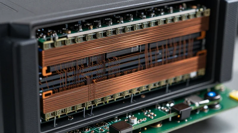
The Architecture of High-Density Interconnects
High-layer count PCBs (typically 12 to 24+ layers) are essential for high-performance server motherboards, allowing for the integration of multi-core CPUs, advanced memory arrays, and high-speed networking controllers. As signal integrity becomes increasingly sensitive to trace length and crosstalk, higher layer counts provide the necessary vertical space for dedicated reference planes, differential pair routing, and isolated power distribution networks.
Impact of Layer Density on Signal Performance
| Feature | Low-Layer Impact | High-Layer Benefit |
|---|---|---|
| Signal Crosstalk | High risk due to congestion | Minimized via isolation planes |
| Power Delivery | Higher impedance drops | Stable voltage via thick planes |
| Thermal Management | Limited spreading layers | Enhanced via heat-dissipating copper |
Key Considerations for Selecting High-Layer Boards
- Why is board registration accuracy critical?
As layer counts increase, the tolerance for interlayer registration decreases; misalignment can cause shorts or signal impedance mismatches that destroy high-speed data integrity. - How does material selection affect performance?
Using high-Tg (glass transition temperature) and ultra-low loss dielectric materials is mandatory to prevent thermal delamination and signal attenuation in high-density stack-ups. - Does higher layer count simplify routing?
While it allows for more routing channels, it significantly increases the complexity of via structures and back-drilling requirements, which are necessary to eliminate signal stubs.
Material Selection: Balancing Dielectric Constant and Loss Tangent
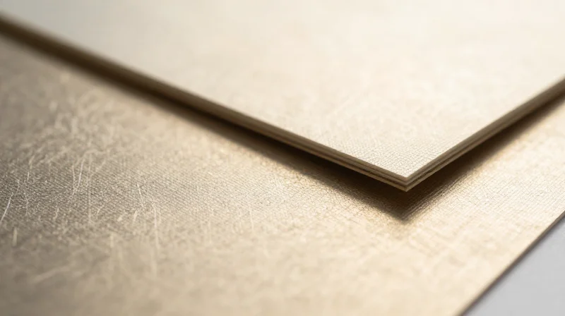
Optimizing Signal Integrity through Material Properties
In high-layer server designs, the primary challenges are minimizing insertion loss and managing impedance control across dense interconnects. Engineers must prioritize low-loss laminates that offer a stable dielectric constant (Dk) across a broad frequency spectrum and a low dissipation factor (Df), also known as the loss tangent. As frequencies push into the 56Gbps and 112Gbps PAM4 territory, even minor fluctuations in material properties can result in catastrophic signal degradation.
Key Laminate Performance Comparison
| Material Grade | Dielectric Constant (Dk) | Loss Tangent (Df) | Primary Application |
|---|---|---|---|
| Standard FR-4 | 4.4 - 4.8 | 0.020 | Low-speed legacy systems |
| Mid-Loss Laminate | 3.8 - 4.0 | 0.010 | 10Gbps enterprise servers |
| Ultra-Low Loss | 3.2 - 3.6 | 0.003 | 112Gbps Data Center Switching |
Critical Selection Factors
- Why is Dk stability important?
A stable Dk ensures that signal velocity remains consistent across the PCB, preventing timing jitters and ensuring that differential pairs maintain accurate phase alignment at high clock rates. - How does Df impact reliability?
The loss tangent directly correlates to signal attenuation. By selecting low Df materials, you reduce the energy lost as heat within the dielectric, which is essential for maintaining signal amplitude over long traces in high-layer count boards. - Does thermal expansion matter?
Yes, high-layer count boards undergo significant thermal cycling. Selecting materials with a low Coefficient of Thermal Expansion (CTE) is vital to prevent via cracking and delamination, which are primary failure modes in server environments.
Mastering Signal Integrity (SI) in Multilayer Boards

As server motherboards push data rates into the 56Gbps and 112Gbps PAM4 regimes, maintaining signal integrity (SI) becomes the primary barrier to reliability. In multilayer architectures, effective SI management is not a single design step but a comprehensive strategy that spans stackup design, routing topology, and electromagnetic compatibility.
Precision Impedance Control and Stackup Design
Impedance discontinuity is the primary source of signal reflections, which degrades eye diagrams in high-speed links. Achieving a consistent 85-ohm or 100-ohm differential impedance requires tight tolerance control during the lamination process. Key strategies include utilizing precise trace width and spacing, but more importantly, managing the proximity to reference planes.
| Parameter | SI Impact | Management Strategy |
|---|---|---|
| Dielectric Thickness | High | Use laser-direct imaging and controlled core materials. |
| Trace Surface Roughness | Medium | Utilize VLP (Very Low Profile) copper foils. |
| Via Stubs | Extreme | Implement back-drilling to eliminate resonant stubs. |
Mitigating Crosstalk and EMI
Crosstalk—the unwanted electromagnetic coupling between parallel traces—is compounded by high layer counts where vertical routing is dense. To mitigate this, engineers must enforce strict '3W' rules and prioritize broadside coupling prevention. In server designs, isolating high-speed differential pairs with interstitial ground stitching vias is essential to prevent edge-fire EMI leakage.
- How does layer stackup affect crosstalk?
Increased layer density reduces the physical distance between signal layers, necessitating more aggressive use of solid ground planes as shields between active layers. - Why is back-drilling critical for server PCBs?
Signal via stubs act as antennas at high frequencies. Back-drilling removes the unused portion of the via barrel, significantly reducing signal attenuation and resonance. - How can ground stitching improve SI?
Placing stitching vias near signal return paths minimizes loop inductance, ensuring a low-impedance path for return currents and minimizing EMI radiation.
Advanced Thermal Management Strategies
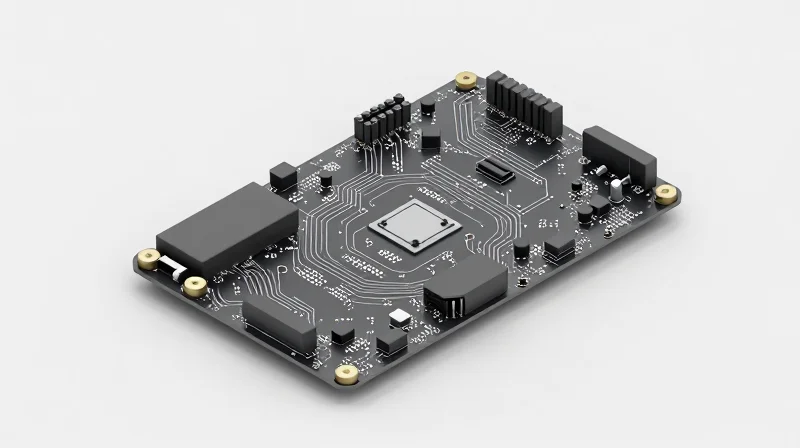
Thermal Management in High-Density Architectures
As server motherboards scale to 12 or more layers, the concentration of high-TDP CPUs and GPUs creates localized thermal zones that threaten system reliability. Effective heat management necessitates a holistic design approach that integrates internal thermal dissipation paths directly into the board stack-up, moving beyond traditional external heat sinks.
Optimizing Thermal Via Arrays
Thermal vias act as primary conduits for heat transfer from the component pad to inner ground and power planes. To maximize efficiency, designers must balance the density of these arrays with manufacturing constraints, such as drill registration accuracy and plating uniformity, to avoid board delamination.
| Via Strategy | Performance Benefit | Design Consideration |
|---|---|---|
| Copper-Filled Vias | Highest thermal conductivity | Requires costly planarization process |
| Standard Plated Vias | Cost-effective solution | Limited vertical heat flow capability |
| VIPPO (Via-in-Pad) | Direct thermal pathing | Needs careful solder mask management |
Advanced Substrate Integration
For extreme heat density, standard FR-4 laminates are often insufficient. Integrating metal-core PCBs (MCPCB) or heavy-copper internal planes facilitates heat spreading, effectively reducing the junction temperature of sensitive silicon components.
- How does layer count impact thermal resistance?
Increased layer counts enable thicker copper planes and more frequent internal ground layers, which act as effective heat spreaders compared to lower-layer count boards. - What are the risks of thermal expansion in high-layer boards?
Differential coefficients of thermal expansion (CTE) between the copper traces, glass fiber, and resin can lead to barrel cracking in vias; choosing materials with matched CTE is vital for data center longevity. - Is metal-core technology necessary for all servers?
No, it is generally reserved for high-TDP specialized server applications where standard cooling methods fail to keep component temperatures within the manufacturer's specified operating range.
The Role of Surface Finish and Copper Weight
In high-layer count server PCBs, the surface finish and copper weight are not merely aesthetic or base-level considerations; they are fundamental determinants of signal integrity, mechanical robustness, and resistance to environmental degradation. Balancing these factors is essential to withstand the thermal cycling inherent in data center environments.
The Impact of Copper Weight on Reliability
Copper weight directly influences thermal dissipation and current-carrying capacity. For high-TDP processors, heavier copper (typically 2oz or higher for internal layers) is often required to minimize I2R losses and prevent localized heating. However, heavy copper complicates the etching process and can affect fine-pitch routing capabilities. Engineers must calculate the precise current requirements for power distribution networks (PDN) to avoid unnecessary complexity that could impede impedance control.
Surface Finish Performance Comparison
| Surface Finish | Reliability | Assembly Suitability | Best Use Case |
|---|---|---|---|
| ENEPIG | Excellent | High (Multi-cycle) | Complex SMT/BGA |
| ENIG | Good | Standard | High-Density Routing |
| Immersion Silver | Moderate | Limited | Cost-Sensitive |
Key Considerations for Assembly and Durability
- How does ENEPIG compare to traditional ENIG?
ENEPIG (Electroless Nickel Electroless Palladium Immersion Gold) offers superior wire bonding and solder joint reliability, effectively mitigating the 'black pad' risks associated with standard ENIG in high-thermal-stress environments. - Does copper weight affect high-speed signal integrity?
Yes; excessively thick copper increases skin effect losses and complicates trace geometry, making it harder to maintain strict impedance tolerances on high-speed differential pairs. - Why is finish selection critical for high-layer counts?
High-layer count boards often undergo multiple reflow cycles; a robust finish like ENEPIG ensures that surface pads remain solderable throughout the entire assembly process without oxidation or interface degradation.
Manufacturing Tolerances and Via Technology
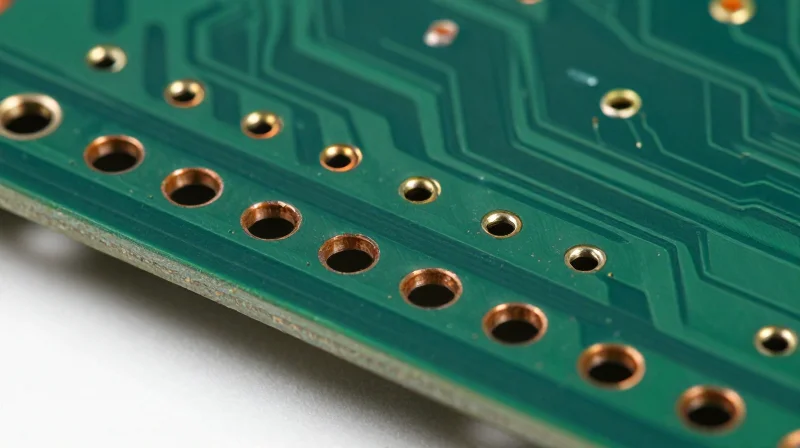
For data center motherboards reaching 12 to 20+ layers, the precision of via structures and manufacturing tolerances is not merely a design preference—it is a functional requirement. As signaling speeds surpass 56Gbps and 112Gbps PAM4, the transition from standard through-hole vias to complex HDI configurations dictates the board's signal integrity and long-term mechanical reliability.
Via Technology: Balancing Density and Signal Integrity
To minimize parasitic capacitance and inductive stubs that degrade high-frequency signals, modern server boards move away from traditional through-hole vias. Designers must evaluate the trade-offs between various via architectures:
| Via Type | Signal Integrity Impact | Cost/Complexity | Primary Application |
|---|---|---|---|
| Through-Hole | High (Stub issues) | Low | Power/Ground Planes |
| Blind/Buried | Medium | Moderate | Layer-to-layer signaling |
| Microvia (HDI) | Excellent | High | High-speed CPU/Memory |
Manufacturing Tolerances: Critical Considerations
In high-layer counts, misregistration of inner layers or inconsistencies in drill-to-copper clearances can lead to catastrophic board failure or intermittent signaling errors. Reliable fabrication relies on strictly managed tolerances.
- Registration Tolerance
Layer-to-layer alignment must typically be maintained within +/- 2 mils for high-speed boards to ensure impedance consistency. - Drill-to-Copper Clearance
As hole density increases, ensuring sufficient annular rings is vital to prevent breakout during thermal expansion cycles. - Aspect Ratio Control
Maintaining an aspect ratio below 10:1 for mechanical drills ensures uniform copper plating, reducing the risk of via barrel cracking.
FAQ: HDI and Reliability
- How do microvias affect thermal cycling performance?
Stacked microvias are more susceptible to fatigue than staggered ones. For high-reliability data center boards, staggered vias are often preferred to distribute mechanical stress. - Why is back-drilling necessary for server boards?
Back-drilling removes the unused portion of a through-hole via (the stub), which acts as an antenna at high frequencies, significantly improving signal integrity.
Quality Assurance and Reliability Testing
Essential Reliability Testing Protocols
To ensure long-term operational integrity, high-layer count motherboards must undergo rigorous validation processes that simulate the aggressive stressors of data center deployment. These tests go beyond standard functional verification, focusing on material stability, interconnection integrity, and electrochemical resilience.
| Test Method | Primary Purpose | Standard Compliance |
|---|---|---|
| Thermal Shock Testing | Evaluates interconnect fatigue under extreme temperature cycling. | IPC-9701 |
| SIR Testing | Measures Surface Insulation Resistance to prevent dendritic growth. | IPC-TM-650 |
| Cross-Section Analysis | Validates barrel fill, plating thickness, and registration accuracy. | IPC-A-600 |
Validating Interconnect Integrity
For boards exceeding 12 layers, the internal via structure is the most common point of failure. Microscopic cross-section analysis is essential to verify that copper plating is uniform within the vias. Voids or thin spots in the plating can result in intermittent connectivity failures once the board is subjected to the thermal expansion associated with high-TDP processor cycles.
Electrochemical Resilience and SIR
Surface Insulation Resistance (SIR) testing is vital for high-density interconnect (HDI) designs. As trace spacing shrinks, the risk of electrochemical migration—where moisture and voltage cause conductive filaments to grow between traces—increases significantly. Validating cleaning processes and material chemical compatibility through SIR testing ensures the board will not suffer from catastrophic short circuits over its multi-year service life.
Frequently Asked Questions
- How many thermal cycles should a server PCB endure?
For high-reliability server applications, boards are typically expected to withstand a minimum of 1,000 thermal cycles between -40°C and 125°C without significant change in electrical resistance. - Is cross-section analysis destructive?
Yes, cross-section analysis requires cutting into a representative sample coupon, making it a destructive test performed on production batch samples rather than the final customer-bound hardware. - Why is SIR testing more important for high-layer boards?
High-layer boards often use advanced materials and high-density routing; any residue from the manufacturing process can trap ions, leading to leakage currents that degrade signal integrity and cause failure in high-humidity environments.
Supply Chain Considerations for Critical Infrastructure
Mitigating Procurement Risks for Critical Infrastructure
For data center operations, the PCB is the foundation of reliability; disruptions in the supply chain or quality drift in volume production pose catastrophic risks to uptime. Procurement must shift from simple cost-based vendor selection to a risk-based framework that mandates deep visibility into the manufacturer's operational maturity, disaster recovery capabilities, and material sourcing stability.
Key Supply Chain Evaluation Metrics
| Risk Factor | Mitigation Strategy | KPI for Selection |
|---|---|---|
| Material Shortages | Vertical integration and multi-sourcing | Raw material inventory levels |
| Capacity Bottlenecks | Diversified production lines | Yield-per-machine consistency |
| Quality Drift | In-line automated optical inspection | DPPM (Defective Parts Per Million) |
Vendor Auditing and Quality Governance
To ensure long-term server durability, vendors must demonstrate robust Quality Management Systems (QMS) beyond basic ISO 9001 compliance. Critical infrastructure providers should prioritize partners that implement total quality control protocols, including lot traceability that links individual PCBs back to specific material batches and production timestamps. This traceability is vital for rapid root-cause analysis in the event of field failures.
- How do we verify a partner's manufacturing capacity?
Conduct site audits focused on equipment age, automation levels, and maintenance schedules to ensure the facility can handle high-layer counts consistently without throughput-induced errors. - What role does geographic location play in supply chain risk?
Geopolitical stability and proximity to high-frequency logistics corridors are critical; decentralized manufacturing footprints are preferred to prevent single-point-of-failure scenarios. - Should we require material provenance data?
Yes. Ensuring the authenticity and consistency of pre-preg and copper-clad laminate sources is essential to maintain impedance control and thermal stability across production runs.
Selecting the right high-layer count PCB is a balance of advanced material physics and rigorous engineering standards. By prioritizing thermal performance, signal integrity, and manufacturing precision, you ensure the long-term reliability of your critical server infrastructure. Ready to upgrade your hardware roadmap? Contact our engineering team today for a consultation on custom PCB procurement solutions.
