
In the world of high-accuracy test and measurement, a PCB is not merely a mounting board; it is a fundamental component of the signal chain. Choosing the wrong architecture can introduce noise, thermal drift, and signal degradation that compromises measurement precision. This guide outlines the essential technical criteria to ensure your hardware meets the most demanding industrial standards.
Understanding the Demands of Precision Instrumentation
Why Precision Instrumentation Demands Higher Standards
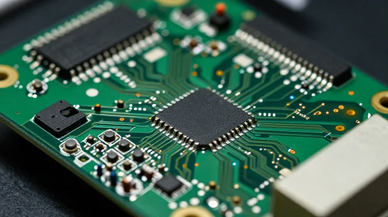
In mission-critical test and measurement systems, the PCB is not merely a mounting platform for components; it is an active participant in signal conditioning and data integrity. Unlike standard consumer electronics, which prioritize cost-reduction and compact integration, instrumentation PCBs must preserve the fidelity of minute electrical signals. Any variation in impedance, thermal gradients, or electromagnetic interference (EMI) can be interpreted as false data, leading to catastrophic failure or inaccurate measurements in critical applications.
Comparative Requirements
| Parameter | Consumer Electronics | Precision Instrumentation |
|---|---|---|
| Signal Fidelity | Low priority; tolerance for noise | Highest priority; absolute signal integrity |
| Thermal Management | Passive cooling; localized heat | Active thermal stability; low-drift materials |
| Dielectric Consistency | Standard FR-4 | High-Tg, low-loss, stable Er materials |
| Layer Stackup | Minimal count | Complex impedance-controlled stacks |
Common Challenges in High-Precision PCB Selection
- How does dielectric absorption affect performance?
In high-precision applications, the dielectric material in the PCB can trap charge, causing memory effects in signal traces. Selecting low-loss materials is essential to minimize signal distortion. - Why is thermal expansion critical?
Uneven Coefficients of Thermal Expansion (CTE) across different board layers can lead to micro-fractures in vias during temperature cycles, resulting in intermittent failures that are notoriously difficult to debug. - How do board finishes influence long-term stability?
The surface finish impacts both solder reliability and oxidation resistance. ENIG or Immersion Silver are preferred over standard HASL to ensure consistent contact resistance and mechanical longevity.
Material Selection: Balancing Dielectric Constant and Loss Tangent

The Dielectric Constant (Dk) Stability Factor
For test and measurement systems, the dielectric constant (Dk) must be stable across temperature, frequency, and humidity variations. Any variation in Dk directly shifts the signal propagation delay, which translates into phase errors in time-domain measurements. Engineers must prioritize laminates with low Dk thermal coefficients, typically utilizing PTFE-based or advanced hydrocarbon ceramic filled materials, to maintain precise timing correlation.
Optimizing Loss Tangent (Df) for Attenuation Control
The loss tangent (Df) or dissipation factor dictates the amount of energy absorbed by the board material, directly impacting signal attenuation. In broadband instrumentation, high insertion loss leads to degraded dynamic range and signal-to-noise ratios. Selecting materials with a low Df is non-negotiable for high-frequency channels where every decibel of signal strength is critical for measurement accuracy.
| Material Class | Typical Dk | Loss Tangent (Df) | Primary Application |
|---|---|---|---|
| Standard FR-4 | 4.4 - 4.8 | 0.020 | Low-frequency control |
| High-Tg/Low-Loss FR-4 | 3.8 - 4.2 | 0.008 - 0.012 | Digital backplanes |
| PTFE/Ceramic Composite | 2.5 - 3.5 | 0.001 - 0.002 | RF/Microwave instrumentation |
Selecting the Right Laminate: FAQ
- How does moisture absorption affect Dk stability?
Moisture ingress increases the effective Dk of a PCB because water has a high dielectric constant (~80). Materials with low moisture absorption rates are essential to maintain consistent impedance in uncontrolled environmental conditions. - Is a lower Dk always better?
While lower Dk reduces parasitic capacitance and allows for wider trace widths for 50-ohm matching, the primary focus for precision instrumentation should be Dk consistency and tolerance rather than just the lowest absolute value. - Why is copper foil surface roughness important?
At high frequencies, the skin effect causes current to flow near the surface of the conductor. Rough copper foil increases resistive losses and degrades phase stability, so choosing low-profile or rolled-annealed copper is critical.
Thermal Stability and Coefficient of Thermal Expansion (CTE)
Thermal Stability and Coefficient of Thermal Expansion (CTE)
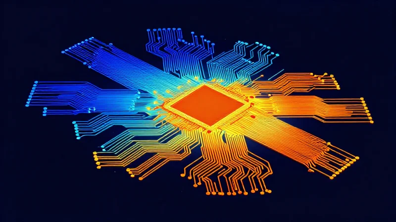
In precision instrumentation, PCB failure is rarely immediate; it is often the result of cumulative fatigue caused by thermal cycling. High-precision systems operate in environments where temperature gradients can cause differential expansion between the copper traces and the dielectric substrate, leading to barrel cracking in vias or delamination. Selecting materials with a low Coefficient of Thermal Expansion (CTE)—specifically matching the Z-axis expansion to that of the copper plating—is vital for preserving electrical connectivity over long-term operation.
Key Thermal Metrics for Material Selection
| Metric | Significance for Precision PCBs | Recommended Target |
|---|---|---|
| Tg (Glass Transition) | Temperature at which resin turns rubbery. | > 170°C |
| Td (Decomposition) | Point of material thermal degradation. | > 340°C |
| Z-Axis CTE | Expansion through board thickness. | < 3% (50-260°C) |
To achieve high-precision results, designers must prioritize laminates that demonstrate minimal CTE mismatch. While standard FR-4 is sufficient for consumer products, its high CTE leads to micro-cracks in through-hole plating when exposed to the intense thermal fluctuations typical of heavy-duty calibration and measurement hardware. Using ceramic-filled or woven-glass reinforced PTFE materials offers significantly better stability, ensuring that the dielectric constant (Dk) does not drift significantly as operating temperatures rise.
- Why does Z-axis CTE matter more than X/Y expansion?
Z-axis expansion directly impacts the reliability of plated through-holes (PTH). If the substrate expands significantly faster than the copper barrel, the mechanical strain will eventually cause the copper to fracture, resulting in intermittent signals or complete system failure. - How does temperature affect signal phase?
Most dielectrics exhibit a change in Dk relative to temperature. If the material lacks thermal stability, the signal propagation delay will fluctuate, leading to phase errors in high-speed timing and measurement applications. - What is the role of Tg?
The Glass Transition temperature (Tg) is the threshold where the laminate's physical properties change. Operating near or above this limit causes rapid degradation of mechanical properties, making high-Tg materials non-negotiable for mission-critical instruments.
Optimizing Layer Stack-Up for Signal Integrity
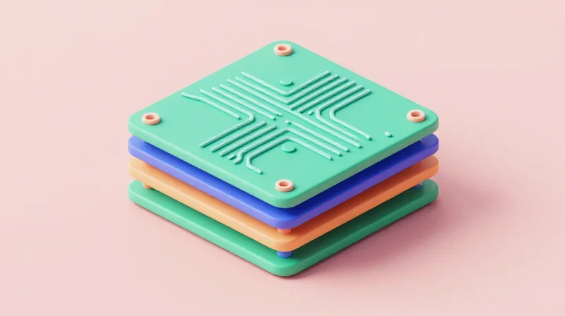
For high-precision instrumentation, the stack-up must be treated as a controlled electromagnetic environment rather than a simple mechanical substrate. Effective signal integrity is achieved by ensuring that every high-speed signal trace has a dedicated, continuous reference plane, thereby minimizing loop inductance and reducing susceptibility to radiated emissions.
Ground Plane Strategy and Return Path Management
The return path is the most critical element of signal integrity. Discontinuities in ground planes—such as those caused by split planes or crossing voids—force return currents to take longer, higher-impedance paths. This creates magnetic loops that radiate noise and inject jitter into sensitive measurement circuits. Use a solid ground plane adjacent to signal layers to ensure low-impedance return paths.
Impedance Matching and Crosstalk Mitigation
Precision instruments rely on strict 50-ohm (single-ended) or 100-ohm (differential) impedance targets. Beyond simple trace width, stack-up design must account for the dielectric thickness between the trace and its reference plane. Increasing the distance between adjacent signal layers, combined with orthogonal routing on signal layers, is essential to minimizing capacitive and inductive crosstalk.
| Strategy | Impact on Signal Integrity | Implementation Best Practice |
|---|---|---|
| Layer Pairing | Reduces Crosstalk | Use S-G-G-S or Signal-Ground-Ground-Signal structures |
| Stitch Vias | Maintains Return Path | Place ground stitching vias near signal layer transitions |
| Dielectric Thickness | Controls Impedance | Specify tight-tolerance prepreg materials |
Common Questions on Stack-up Optimization
- Why is a 6-layer board often the minimum for instrumentation?
A 6-layer stack-up (Signal-GND-Signal-Power-GND-Signal) allows for dedicated reference planes for every signal layer, providing the shielding necessary to prevent digital noise from contaminating precision analog measurement paths. - Should I use buried vias in high-precision boards?
Buried and blind vias can help reduce parasitic capacitance and inductance of via stubs. However, they increase manufacturing complexity and cost. They are recommended only when signal speeds exceed 5-10 Gbps or when board space for high-density routing is severely limited. - How does stack-up symmetry affect reliability?
Stack-up symmetry is vital for preventing board warp during reflow soldering. An asymmetric stack-up can induce mechanical stress, which may cause micro-cracks in traces or vias, leading to intermittent failure in mission-critical environments.
Mitigating EMI and Noise Injection in Mixed-Signal Boards
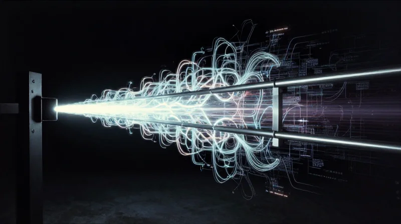
In high-precision instrumentation, the primary challenge is preventing digital switching noise from infiltrating sensitive analog measurement paths. Successful designs treat the PCB as a complex radio-frequency system, where board layout and return-path control are just as critical as the semiconductor selection itself.
Strategic Partitioning and Grounding
Physical separation remains the first line of defense. Analog and digital domains must be physically segregated, with components placed to prevent trace proximity that could induce capacitive coupling. For return paths, a single solid ground plane is often superior to split planes, provided that high-speed signals are routed exclusively over the reference plane without crossing over gaps or discontinuities, which can create significant EMI loops.
Comparison of EMI Mitigation Techniques
| Technique | Primary Benefit | Implementation Difficulty |
|---|---|---|
| Physical Partitioning | Reduces direct crosstalk | Low |
| Shield Cans (Faraday) | Blocks radiated EMI | Medium |
| Differential Signaling | Common-mode noise rejection | High |
| Guard Traces/Vias | Reduces edge coupling | Medium |
FAQ: Noise Management in Mixed-Signal Design
- Should I use split ground planes for analog and digital sections?
Modern high-speed design favors a continuous ground plane to control return path impedance, provided you maintain strict physical separation of components. Splitting planes often leads to unintentional slot antennas if routing crosses the gap. - How do I mitigate noise injection from power rails?
Use dedicated ferrites and low-ESR decoupling capacitors localized to each IC's power pin, while ensuring the power distribution network (PDN) has low impedance across the frequency band of the measured signals. - Is board-level shielding necessary for all high-precision boards?
Shielding is essential if the board is near high-frequency digital processors or radio interfaces. It creates a controlled environment for the sensitive analog front-end by attenuating radiated interference.
Navigating Regulatory Compliance and Certification Standards
For mission-critical instrumentation, PCB design and manufacturing must transcend standard commercial practices to achieve rigorous industry certifications. Adherence to these standards is not merely a legal obligation for market entry but a technical baseline that ensures long-term operational integrity, safety, and electromagnetic compatibility (EMC) in volatile industrial or research environments.
Essential Industry Standards and Compliance Frameworks
| Standard Body | Key Standard | Primary Focus |
|---|---|---|
| IPC | IPC-6012 Class 3 | High-reliability performance requirements for rigid PCBs. |
| ISO | ISO 9001:2015 | Quality management system requirements for manufacturing consistency. |
| IEC | IEC 61010-1 | Safety requirements for electrical equipment for measurement and lab use. |
| UL | UL 796 | Standard for printed wiring boards, focusing on material flammability and safety. |
Navigating Global Safety Mandates
To deploy instrumentation globally, manufacturers must satisfy regional safety protocols. In North America, UL (Underwriters Laboratories) certification is often the prerequisite for electrical safety. In the European Union, CE marking requires compliance with the Low Voltage Directive (LVD) and the Electromagnetic Compatibility (EMC) Directive. Failure to verify these standards early in the design cycle can lead to costly late-stage re-designs or restricted market access.
Frequently Asked Questions
- Why is IPC-6012 Class 3 critical for mission-critical instruments?
Class 3 provides the highest level of inspection and acceptance criteria, ensuring the board can withstand harsh, continuous-duty environments where downtime is unacceptable. - How does RoHS and REACH compliance impact PCB selection?
These environmental directives mandate the elimination of hazardous substances like lead and brominated flame retardants, requiring the use of lead-free compatible high-Tg substrates. - What role does ISO 13485 play if the instrumentation is medical?
If your test equipment is used for medical diagnostics, compliance with ISO 13485 is often mandatory, enforcing strict documentation, traceability, and risk management throughout the PCB manufacturing cycle.
Choosing the Right PCB Manufacturing Partner
For mission-critical test and measurement instrumentation, the PCB fabrication partner is an extension of your engineering team. High-precision requirements demand more than just standard manufacturing tolerances; they require a partner capable of advanced material handling, rigorous automated optical inspection (AOI), and process stability that ensures consistent impedance control across production runs.
Critical Evaluation Criteria for High-Precision Fabrication
| Evaluation Criterion | Requirement for High-Precision | Why It Matters |
|---|---|---|
| Material Handling | Low-loss laminates (e.g., Rogers, Megtron) | Maintains signal integrity at high frequencies. |
| Registration Accuracy | +/- 1-2 mil layer alignment tolerance | Prevents via-pad breakout and layer shifts. |
| Quality Certification | AS9100, ISO 13485, IPC Class 3 | Ensures traceability and process reliability. |
| Test Infrastructure | Flying probe and Bed-of-Nails testing | Validates connectivity in high-density nets. |
Frequently Asked Questions
- How do I verify a manufacturer's claims of precision?
Request a First Article Inspection (FAI) report and sample data from previous builds similar to your layer count and technology complexity. Auditing their AOI and X-ray inspection logs provides proof of process control. - Is IPC Class 3 certification always necessary?
For mission-critical instrumentation where failure results in significant loss or safety risks, IPC Class 3 is highly recommended. It mandates tighter tolerances and more stringent inspection criteria than the standard Class 2. - Why should I prioritize a partner with in-house impedance testing?
External impedance testing increases lead times and introduces handling risks. A partner with in-house Time Domain Reflectometry (TDR) equipment ensures that your design's impedance requirements are verified on every production batch.
Risk Mitigation and Supply Chain Stability
Beyond technical specifications, assess the financial health and supply chain transparency of the manufacturer. For instruments with long lifecycles, ensure the partner has robust document control systems to manage revision changes and material obsolescence. A reliable partner should proactively communicate potential design-for-manufacturing (DFM) risks early in the quoting phase, rather than forcing design changes during the fabrication stage.
Selecting the right PCB architecture is the difference between reliable data and measurement failure. By focusing on thermal stability, high-performance materials, and rigorous signal integrity, you ensure your equipment delivers consistent accuracy. Ready to elevate your design? Contact our engineering team today for a technical consultation on your next project.
