
In the fast-evolving landscape of connected vehicles, the telematics gateway serves as the mission-critical heart of automotive communication. As data throughput increases and electromagnetic interference grows, engineers must balance signal integrity with rugged reliability. This guide provides a strategic framework for selecting the right substrate and stack-up architecture to ensure your telematics hardware excels in harsh automotive environments.
Understanding the Automotive Telematics Environment

The Demanding Automotive Telematics Ecosystem
Automotive telematics gateways are the central nervous system for modern connected vehicles, facilitating V2X (Vehicle-to-Everything) communication, OTA updates, and real-time fleet diagnostics. Unlike standard consumer electronics, these components operate within a high-stakes, physically punishing environment. Selecting a multi-layer PCB for these applications requires more than standard performance metrics; it demands a robust understanding of thermal dissipation, mechanical resilience, and electromagnetic compatibility.
Environmental Stress Factors
| Stress Factor | Typical Operational Constraint | Impact on PCB Reliability |
|---|---|---|
| Temperature | -40°C to +125°C | CTE mismatch leading to solder joint fatigue |
| Vibration | Broadband random vibration | Interconnect cracking and delamination |
| Electromagnetic Interference | High-density RF switching | Signal crosstalk and data corruption |
Key Considerations for Gateway Reliability
- How do thermal fluctuations impact high-speed signal integrity?
Extreme temperature swings alter the dielectric constant (Dk) of PCB substrate materials, which can lead to impedance shifts in high-speed traces, potentially causing signal reflections or increased bit error rates in high-frequency data lanes. - Why is mechanical vibration a primary failure vector?
Continuous mechanical stress from road conditions can degrade the via-to-pad interfaces. For multi-layer boards, selecting high-TG (glass transition temperature) laminates is essential to maintain structural stability under constant vibration cycles. - What is the primary challenge regarding high-frequency noise?
With multiple protocols like 5G, DSRC, and GNSS operating simultaneously, the gateway board faces significant near-field crosstalk. Strategic layer stack-up and proper shielding are required to prevent noise coupling between analog RF circuits and digital logic layers.
Material Selection: Beyond Standard FR-4
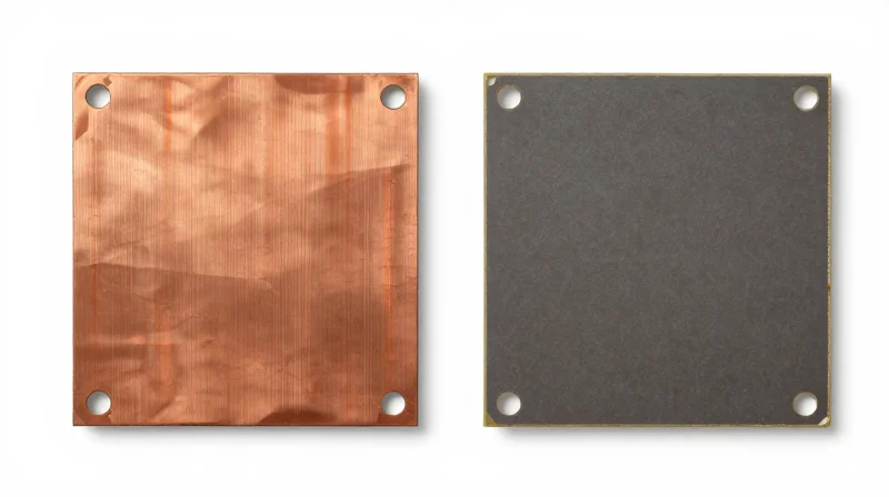
Standard FR-4 is insufficient for modern high-speed automotive telematics due to its inconsistent dielectric constant (Dk) and relatively high dissipation factor (Df) at frequencies exceeding 2 GHz. As data rates for V2X (Vehicle-to-Everything) communications scale, engineers must transition to high-frequency, low-loss laminate materials that offer stable electrical performance across wide temperature ranges and high moisture resistance.
Performance Comparison: Standard FR-4 vs. High-Speed Laminates
| Material Property | Standard FR-4 | High-Speed Laminate | Impact on Telematics |
|---|---|---|---|
| Dielectric Constant (Dk) | 4.4 - 4.8 | 3.2 - 3.8 | Reduces signal propagation delay |
| Dissipation Factor (Df) | 0.020 | <0.005 | Lowers signal attenuation/insertion loss |
| Glass Transition (Tg) | 130-140°C | 170-200°C | Enhanced thermal/mechanical stability |
Key Material Selection Criteria
When moving away from FR-4, the selection process should prioritize materials that mitigate signal dispersion while surviving harsh under-the-hood environments.
- Dk and Df Stability
Choose materials with a flat Dk/Df curve relative to frequency and temperature to prevent impedance mismatches and unpredictable signal timing during engine ignition cycles. - Thermal Reliability (Tg and Td)
Prioritize high Glass Transition Temperature (Tg) and Decomposition Temperature (Td) to ensure the board resists delamination and copper trace lifting during thermal cycling. - Moisture Absorption
Select substrates with low moisture absorption (typically <0.1%) to prevent dielectric property shifts caused by automotive humidity fluctuations. - Copper Foil Surface Profile
Utilize Very Low Profile (VLP) or Hyper-Low Profile (HVLP) copper to minimize the skin effect at high frequencies, further reducing insertion loss in high-speed traces.
Optimizing Multi-Layer Stack-up Architectures

Strategic Layer Assignment for Signal Integrity
To achieve optimal signal performance, engineers must prioritize a symmetrical stack-up design that utilizes dedicated ground planes adjacent to high-speed signal layers. This configuration minimizes loop areas and provides a controlled return path, which is fundamental in mitigating common-mode noise in telematics applications.
| Layer Type | Strategic Purpose | Best Practice |
|---|---|---|
| Signal Layer | High-speed data transmission | Route on inner layers between ground planes |
| Reference Plane | Return path & EMI shielding | Maintain low-impedance ground reference |
| Power Plane | Voltage distribution | Decouple locally to reduce transient noise |
Impedance Control and Crosstalk Mitigation
Impedance consistency is critical when operating above 1 Gbps. Designers should leverage trace width calculations based on dielectric thickness and permitivity while strictly adhering to the 3W rule (trace separation equals three times the trace width) to significantly reduce capacitive crosstalk between adjacent high-speed differential pairs.
Common Implementation Questions
- Why is layer symmetry vital?
Symmetry prevents mechanical warpage during thermal cycling in automotive environments and ensures balanced electrical characteristics across the board. - How does power plane distribution affect noise?
Splitting power planes can inadvertently create return path discontinuities; ensure planes are contiguous beneath high-speed signal runs to prevent EMI radiation. - Is buried via technology necessary?
While more costly, buried and blind vias reduce signal stub length, which is crucial for minimizing signal reflections at multi-gigahertz data rates.
Signal Integrity (SI) Challenges in Gateway Gateways
Automotive telematics gateways serve as the nerve center for V2X communications, handling high-speed data streams that are exceptionally sensitive to signal degradation. As frequencies climb into the multi-gigahertz range, even minor discontinuities in the transmission line can result in significant eye diagram closure, increased jitter, and bit error rate (BER) spikes. Engineers must move beyond standard layout techniques, prioritizing electromagnetic compatibility (EMC) through advanced via optimization, strict differential pair control, and disciplined return path management.
Critical Mitigation Strategies
- Via Optimization
Implement back-drilling to remove unused via stubs, which act as resonant structures at high frequencies. Use ground stitching vias adjacent to signal transitions to maintain a consistent reference plane transition. - Differential Pair Integrity
Ensure intra-pair skew is minimized during trace routing to prevent mode conversion. Maintain tight coupling while adjusting spacing to achieve target differential impedance, typically 100 ohms. - Return Path Continuity
Prevent signals from crossing splits in reference planes. A clean, unbroken return path is essential to minimizing the loop area, which reduces radiation and inductive coupling.
Comparison of SI Design Approaches
| Technique | Primary Benefit | Complexity Level |
|---|---|---|
| Back-drilling | Reduced stub resonance | High |
| Ground Stitching | Lower return path inductance | Medium |
| Loose vs. Tight Coupling | Impedance control vs. Crosstalk | Low |
Design Best Practices for Automotive Gateways
Rule 1: Never route high-speed signals across split reference planes.
Rule 2: Use 3W spacing rule for trace-to-trace crosstalk isolation.
Rule 3: Ensure consistent reference plane transition with stitching vias.
Rule 4: Utilize low-loss dielectric materials to minimize attenuation.
Thermal Management and Power Density Considerations

Thermal Management Strategies for Compact Gateways
As automotive telematics gateways transition toward higher power densities and smaller form factors, the traditional reliance on passive convective cooling is insufficient. Engineers must leverage the PCB stack-up itself as a primary thermal conduit. By integrating thermal management into the early layout stages, designers can mitigate hotspots that threaten signal integrity and device longevity.
Key Dissipation Techniques
- Thermal Via Arrays
Utilize thermal via stitching directly beneath high-power components to transfer heat to internal ground planes, which act as large-surface-area heat sinks. - Copper Weight Optimization
Increase outer and internal layer copper weight to 2oz or higher in high-current path regions to lower resistive losses and improve bulk thermal conductivity. - Strategic Component Placement
Isolate high-heat-generating components such as cellular modems and processors away from heat-sensitive oscillators and precision analog front-ends.
Material Impact on Thermal Performance
| Parameter | Standard FR-4 | High-Tg/Thermal Laminate |
|---|---|---|
| Thermal Conductivity | Low (0.25 W/mK) | Improved (>0.5 W/mK) |
| Tg (Glass Transition) | 130°C - 140°C | 170°C - 200°C |
| CTE-Z Axis Stability | Poor | Excellent (Lower Z-expansion) |
Designing for High Power Density
Maximizing power density requires minimizing impedance in power delivery networks (PDN). By utilizing internal plane pairs and minimizing the distance between power and ground layers, designers reduce inductance, which concurrently lowers heat generation. Implementing wide, short traces for current-heavy nets is essential to maintaining thermal stability without sacrificing high-speed signaling performance.
EMI/EMC Compliance and Shielding Techniques
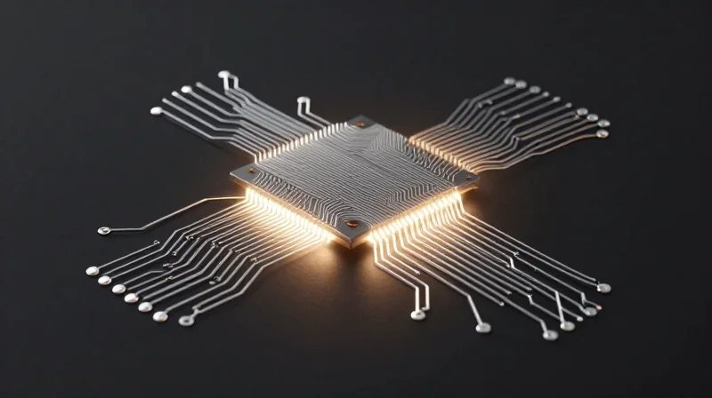
Mitigating EMI in High-Speed Automotive Gateways
Automotive telematics gateways operate in an electrically hostile environment characterized by significant radiated and conducted noise. To ensure compliance with CISPR 25 and ISO 11452 standards, design engineers must prioritize current return path continuity and minimize loop areas across all high-frequency signal layers. Integrating high-speed digital processing with wireless communication modules requires a design strategy that emphasizes strict separation of noisy switching circuits from sensitive RF and analog interfaces, preventing cross-domain interference.
Shielding and Isolation Techniques
| Shielding Method | Primary Application | Effectiveness |
|---|---|---|
| Board-Level Shields (BLS) | RF/Wireless Transceivers | High (Near-field suppression) |
| Faraday Cages/Gaskets | Gateway Enclosures | High (External radiation) |
| Stitching Vias | Internal Layer Transitions | Moderate (Crosstalk reduction) |
Effective shielding often involves a hybrid approach. For internal EMI coupling, the use of continuous ground planes and periodic via stitching—often called 'via fencing'—is essential to contain the electromagnetic field within the transmission line structures. For external compliance, board-level metallic enclosures must be carefully grounded to the chassis or the reference ground plane to prevent resonance and leakage at higher harmonic frequencies.
Compliance Frequently Asked Questions
- How does layer stack-up affect EMI compliance?
A symmetrical stack-up with dedicated ground planes adjacent to signal layers ensures a clear return path, which minimizes the loop area and significantly reduces common-mode radiation. - Why are common-mode filters essential in gateway design?
Common-mode filters are required at the interface of high-speed data lines to suppress noise generated by asymmetric signal transitions that would otherwise violate CISPR 25 radiated emission limits. - What role does chassis grounding play?
Chassis ground acts as a secondary path for noise drainage; however, it must be carefully isolated from signal ground to prevent ground loops that could introduce instability or damage to sensitive low-voltage silicon.
Meeting Automotive-Grade Industry Standards
Core Industry Standards for Telematics Gateways
Automotive telematics gateways serve as critical communication hubs, meaning they must withstand extreme thermal cycling, vibration, and electromagnetic interference. Design engineers must ensure that every PCB material and component stack-up complies with recognized industry benchmarks. Failure to meet these standards often results in delayed production or, more critically, safety recalls.
| Standard | Primary Focus | Impact on PCB Selection |
|---|---|---|
| AEC-Q100 | Component Stress Test | Dictates high-temp operating grade requirements for active devices. |
| ISO 26262 | Functional Safety | Requires strict traceability, documented failure modes, and layout redundancy. |
| IPC-6012 | Rigid PCB Qualification | Defines performance classes for Class 3 boards used in automotive critical systems. |
Material Selection and ISO 26262 Compliance
ISO 26262 mandates that electronic systems operate correctly under all defined conditions, assigning an Automotive Safety Integrity Level (ASIL) to the gateway. When selecting substrates, materials must have a high Glass Transition Temperature (Tg) and a low Coefficient of Thermal Expansion (CTE) to prevent delamination or via cracking during the harsh lifecycles typical of automotive environments. Designers must also maintain comprehensive material documentation for auditability.
- How does AEC-Q100 influence my PCB layout?
AEC-Q100 ensures that silicon devices can operate in Grade 1 or Grade 0 temperature ranges, which requires the PCB layout to support superior thermal dissipation paths through heavy copper pours and optimized thermal vias. - Why is IPC-6012 Class 3 important for telematics?
Class 3 standards mandate higher criteria for plating thickness, drill registration, and inspection, ensuring that telematics gateways do not suffer from intermittent signal failures during vibration-heavy transit. - What documentation is required for safety audits?
You must maintain full traceability for all raw materials, substrate certificates of conformance, stack-up modeling reports, and thermal simulation results to meet ISO 26262 regulatory requirements.
The Role of DFM (Design for Manufacturing) in Reliability
Integrating DFM into High-Speed PCB Architectures
For automotive telematics gateways, DFM is not an afterthought but a foundational phase that dictates the reliability of high-speed data paths. As complexity increases, the margin for fabrication variance shrinks. Implementing DFM early prevents common issues such as trace impedance deviations, solder bridging, and via-in-pad reliability failures during reflow. By aligning the design with the specific capabilities of your fabrication partner, you ensure that high-frequency performance metrics—achieved during simulation—are physically reproducible at mass-production volumes.
Critical DFM Parameters for Reliability
| Parameter | Reliability Impact | DFM Best Practice |
|---|---|---|
| Aspect Ratio | Plating consistency in high-speed vias | Keep aspect ratio under 10:1 for standard drills |
| Copper Balancing | Prevents board warping during thermal cycling | Ensure >80% copper symmetry across layers |
| Annular Ring | Reduces risk of open circuits under stress | Maintain minimum 5-8 mil registration tolerance |
| Surface Finish | Impacts solder joint fatigue life | Use ENIG or ENEPIG for fine-pitch BGA reliability |
DFM Frequently Asked Questions
- How does DFM affect signal integrity?
DFM guidelines minimize manufacturing tolerances that alter dielectric constants or trace geometry, which in turn preserves the intended high-frequency impedance profile of the gateway. - Why is layer stackup symmetry critical in automotive?
Automotive environments subject gateways to wide temperature swings; asymmetric stackups lead to mechanical stress and delamination, which can degrade signal performance over the vehicle's lifespan. - When should DFM analysis begin?
DFM should be performed iteratively during the schematic capture and initial layout phases to avoid costly late-stage redesigns required by fabrication limitations.
Selecting the correct PCB substrate and stack-up is not just a design choice—it is a commitment to vehicle safety and reliability. By prioritizing material properties, thermal performance, and strict adherence to automotive standards, you can future-proof your telematics gateways against the most demanding interference scenarios. Ready to optimize your automotive design? Contact our engineering team today to discuss your next high-performance gateway project.
