
In the race toward miniaturization, Any-Layer HDI PCBs have become the backbone of modern high-performance electronics. Yet, the leap from design to mass production is fraught with risks. Choosing the wrong partner can lead to catastrophic signal loss, thermal issues, and supply chain bottlenecks. This guide provides the strategic framework you need to select a manufacturing partner that transforms your complex design into a reliable, scalable reality.
Evaluating Advanced Microvia Capabilities
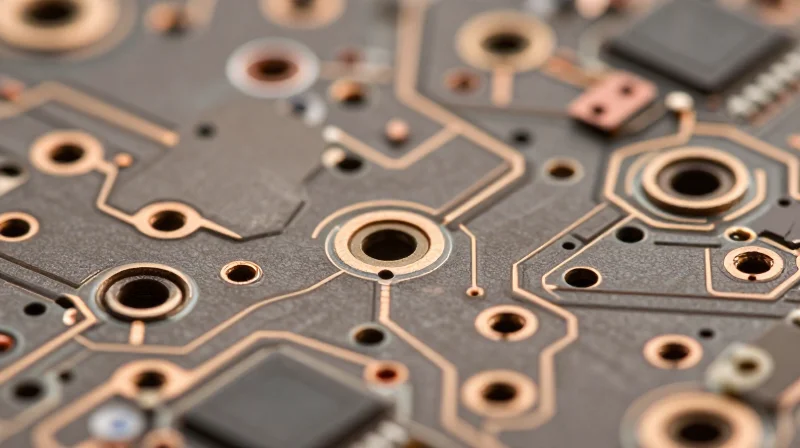
Assessing Laser Drilling Precision
The foundation of reliable any-layer HDI lies in the precision of laser microvia formation. Manufacturers must demonstrate sub-mil accuracy in beam positioning and pulse control to prevent damage to underlying dielectric materials or landing pads. You must request cross-section analysis reports that verify controlled depth and taper geometry, as irregular hole walls can lead to incomplete copper coverage during the metallization phase.
Evaluating Plating Consistency
In stacked microvia structures, copper plating consistency is the primary safeguard against vertical interconnect defects. Voids, inclusions, or variations in plating thickness within the microvia barrel create thermal stress points. An ideal manufacturing partner employs advanced pulse-plating chemistry and real-time bath monitoring to ensure the 'filling' of microvias meets IPC-6012 Class 3 requirements for vertical reliability.
| Metric | Target Specification | Evaluation Method |
|---|---|---|
| Registration Accuracy | +/- 25 microns | X-ray alignment check |
| Microvia Taper | 5 to 10 degrees | Cross-section SEM imaging |
| Copper Plating Voids | Zero tolerance | Dye and pry / Thermal cycling |
Frequently Asked Questions
- How does laser type influence microvia quality?
CO2 lasers are typically used for dielectric ablation, while UV/YAG lasers offer superior precision for smaller vias and copper cutting, minimizing the heat-affected zone (HAZ). - Why is 'stacking' harder than 'staggering'?
Stacked microvias require perfect planarization and precise plating levels to ensure that the contact surface for the next layer is entirely flat, preventing potential cracking during thermal expansion. - What evidence should I request during an audit?
Request historical Cpk data for microvia drilling registration and third-party reliability testing reports covering multiple thermal shock cycles.
Material Science Expertise and Dielectric Selection
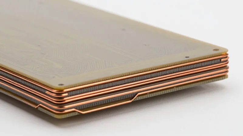
Material Science and Dielectric Selection
In Any-Layer HDI construction, the dielectric material acts as more than just an insulator; it is a critical component of the transmission line geometry. For dense, compact designs, you must partner with a manufacturer who understands the interplay between thermal expansion, signal loss, and copper adhesion. Failing to account for specific material properties can lead to impedance discontinuities and reliability failures, particularly under high thermal loads.
Core Material Considerations for High-Performance HDI
| Parameter | Importance for HDI | Recommendation |
|---|---|---|
| Glass Transition (Tg) | Thermal stability for multi-cycle lamination | High-Tg (>170°C) materials |
| Dissipation Factor (Df) | High-frequency signal integrity | Low-loss laminates (Ultra-low/Very-low) |
| CTE Z-Axis | Preventing barrel cracking in microvias | Low Z-axis expansion resins |
Frequently Asked Questions on Material Selection
- Why is 'High-Tg' material non-negotiable for Any-Layer HDI?
Any-Layer HDI processes involve multiple lamination cycles. A high glass transition temperature ensures the board remains dimensionally stable throughout the manufacturing process, preventing registration errors and delamination. - How does surface roughness impact high-speed performance?
The copper-foil surface roughness (Rz) significantly influences signal loss at high frequencies due to the skin effect. Advanced manufacturers will offer ultra-low-profile copper options to minimize these losses in high-frequency data traces. - What should I look for in a manufacturer's material library?
A qualified partner should provide comprehensive datasheets including dielectric constant (Dk) stability, thermal cycling test results, and proven compatibility with laser-drilling and plating processes specific to your HDI stack-up.
Quality Assurance and Certification Standards
For compact electronic designs, the integrity of an any-layer HDI PCB is entirely dependent on the manufacturer's ability to maintain tight tolerances and process consistency. Because these boards involve high-density interconnects and complex microvia stacking, a robust quality management system (QMS) must be deeply integrated into every stage of the fabrication cycle. Selecting a partner without verified certifications and stringent QA protocols introduces unacceptable risks regarding signal loss, thermal failure, and early-field degradation.
Critical Industry Standards and Certifications
Manufacturers should demonstrate compliance with global standards that specifically address the challenges of HDI technology. While general manufacturing certifications are standard, you must prioritize those that prove technical proficiency in high-density fabrication.
| Certification/Standard | Relevance to HDI PCBs |
|---|---|
| ISO 9001:2015 | Foundational quality management for consistent production processes. |
| IPC-6012 Class 3 | Mandatory for high-reliability electronics where failure is unacceptable. |
| IATF 16949 | Essential for automotive-grade HDI designs requiring zero-defect culture. |
| AS9100 | Required for aerospace applications involving high-thermal stress boards. |
Verifying Quality Control through Environmental Testing
Beyond documentation, your manufacturer must perform in-house environmental and reliability testing. For any-layer HDI, the Coefficient of Thermal Expansion (CTE) mismatch between dielectric materials and copper microvias is a primary failure point. Ensure the manufacturer employs thermal cycling and stress testing to validate the resilience of these connections.
- How do I verify IPC Class 3 adherence?
Request audit reports specifically for Class 3 compliance, focusing on copper wrap thickness in microvias and annular ring requirements. - Is environmental testing standard for all runs?
High-end manufacturers perform destructive physical analysis (DPA) and thermal shock testing on periodic batch samples to ensure process stability. - Why is ISO 14001 important for HDI manufacturing?
Beyond environmental policy, it reflects a disciplined management of chemical processes—critical for the clean etching and plating required in HDI fine-line geometries.
Assessing DFM (Design for Manufacturing) Support
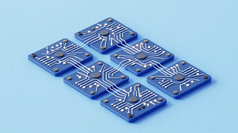
Integrating DFM Early to Optimize Fabrication Yields
Design for Manufacturing (DFM) is not merely a checklist; it is an active engineering partnership. For Any-Layer HDI designs—which rely on complex microvia stacking—engaging your manufacturer’s DFM team during the schematic capture and layout phase is mandatory. Early intervention identifies potential issues like aspect ratio violations, pad-in-via clearance conflicts, and copper balance concerns before they manifest as critical fabrication failures or increased scrap rates.
Critical DFM Collaboration Metrics
| DFM Focus Area | Impact on Design | Why Early Review Matters |
|---|---|---|
| Microvia Stacking | Vertical Interconnect Reliability | Prevents plating voids and inner-layer separation. |
| Copper Distribution | Impedance & Thermal Stability | Reduces stress-related warpage during reflow. |
| Registration Tolerances | Layer Alignment | Maximizes capture pad yield in dense high-pin-count BGA. |
Evaluating Manufacturer DFM Capabilities
- Do they offer custom design rule checking (DRC)?
A high-tier manufacturer provides custom DRC files tailored to their specific laser drilling and plating processes, rather than relying on generic industry-standard rules. - How do they handle DFM feedback reports?
Look for manufacturers that provide detailed, interactive reports highlighting specific design improvements for drill-to-copper distances and annular ring optimization. - Are their DFM engineers accessible?
The best partners offer direct access to front-end engineering staff who can interpret stack-up simulations and advise on material-specific constraints.
By moving beyond simple file validation and fostering a technical dialogue, you ensure that your Any-Layer HDI design is not just manufacturable, but optimized for cost-efficiency and field-proven reliability. A proactive DFM approach is the single most effective way to shorten time-to-market for complex compact electronics.
Manufacturing Scalability and Throughput

Bridging the Gap from NPI to Mass Production
The transition from New Product Introduction (NPI) to high-volume production is often where complex HDI designs fail. A qualified partner must demonstrate a scalable infrastructure that maintains the exact registration tolerances and laser-drilling precision used in prototypes when moving to large-panel, high-output production lines. Look for manufacturers that utilize automated optical inspection (AOI) integrated directly into the plating and drilling stages to catch deviations before they manifest as yield-killing defects.
Scalability Metrics: Prototyping vs. High-Volume
| Metric | NPI Focus | Volume Production Focus |
|---|---|---|
| Registration | Manual Alignment | Automated X-Ray Drilling |
| Material Handling | Small Panel/Coupon | Large Format Automation |
| Inspection | 100% Manual AOI | AI-Enhanced High-Speed AOI |
| Throughput | Agile/Low Volume | Stable Yield/High Volume |
Maintaining Yield Consistency
Yield stability is the most critical KPI when scaling any-layer HDI PCBs. Because these designs utilize micro-vias and stacked-via structures, even minor process fluctuations in the copper plating or via-fill chemistry can lead to hidden delamination or signal discontinuities. Ensure your partner employs Statistical Process Control (SPC) across all key manufacturing steps to monitor process drift in real-time.
- How do you verify a manufacturer's capacity?
Request a tour of their production floor to observe the ratio of automated vs. manual equipment and ask for their historical yield data specifically for HDI designs with 4+ lamination cycles. - Does higher volume sacrifice precision?
It shouldn't if the manufacturer uses laser direct imaging (LDI) and laser drilling platforms that share the same data files as the prototype runs, ensuring absolute consistency regardless of the volume. - What role does supply chain agility play?
A scalable manufacturer maintains deep buffer stocks of the specialized high-frequency, low-loss laminates required for your design, preventing lead-time spikes during production ramp-ups.
Supply Chain Transparency and Lead Time Reliability
Any-layer HDI PCBs rely on specialized materials—such as ultra-thin core laminates and advanced resin systems—that are sensitive to supply chain fluctuations. A manufacturer's ability to maintain a transparent, resilient supply chain directly impacts your project's ability to reach the market on schedule. You must partner with manufacturers that demonstrate proactive inventory management and granular visibility into their procurement tiers.
Evaluating Sourcing Strategies and Material Resilience
Not all manufacturers manage material risks equally. A top-tier provider should maintain dual-sourcing strategies for critical materials, particularly for the specialized build-up layers unique to any-layer HDI designs. During your vetting process, request documentation on how they manage 'force majeure' events and their history of engaging with long-lead-time material suppliers.
| Sourcing Metric | Low-Risk Indicator | High-Risk Indicator |
|---|---|---|
| Material Diversification | Multiple qualified vendors for all build-up layers | Single-source dependency for core laminates |
| Inventory Buffer | Predictive stock levels based on historical NPI data | Just-in-time ordering upon receipt of PO |
| Transparency Level | Real-time portal access to material status | Manual updates requiring weekly status calls |
Assessing Lead Time Predictability
- How do I verify their actual lead time performance?
Ask for 'On-Time Delivery' (OTD) metrics specifically for any-layer HDI projects over the past four quarters. A reliable manufacturer will openly discuss their capacity utilization rates and how they prioritize scheduled production slots versus rush orders. - What indicates a lack of transparency regarding delays?
Beware of providers who only communicate delays once the expected delivery date has passed. A transparent partner will notify you the moment a potential constraint is identified, providing a revised schedule and potential mitigation paths. - Does geographic location matter for lead times?
Yes. While global supply chains offer lower costs, they increase logistics risks. Evaluate if the manufacturer has localized stocking hubs or regional logistics partners that can buffer against cross-border delays.
Ultimately, your manufacturer should function as an extension of your procurement team. By demanding transparency in their material sourcing and holding them accountable to historical lead time performance data, you effectively reduce the risk of critical project delays in your compact electronic design lifecycle.
Post-Production Support and Failure Analysis

The complexity inherent in Any-Layer HDI designs necessitates a partner who views delivery as the beginning of the relationship rather than the end. When a failure occurs, the speed and technical depth of a manufacturer’s root cause analysis (RCA) directly impact your market reputation and product lifecycle costs.
Evaluating Failure Analysis Capabilities
A world-class PCB partner must offer comprehensive diagnostic capabilities. You should confirm whether they maintain internal cross-sectioning laboratories, SEM (Scanning Electron Microscopy) capabilities, and specialized testing equipment to identify latent defects like microvia fractures or internal delamination.
| Analytical Capability | Importance for Any-Layer HDI | Expected Deliverable |
|---|---|---|
| Micro-sectioning | High | Verification of via-to-pad alignment |
| X-Ray Inspection | Critical | Non-destructive void detection |
| Thermal Stress Testing | High | Evaluation of material CTE mismatch |
| C-SAM Analysis | Medium | Detection of internal interface delamination |
Warranty Protocols and Liability
Beyond technical diagnostics, your manufacturer must have transparent liability and replacement policies. For Any-Layer HDI components, failures are often attributed to complex processes rather than simple material issues, making clear contractual definitions of 'workmanship' versus 'design-induced' failure essential.
- How do we define failure accountability?
Establish a clear protocol distinguishing between manufacturing defects, assembly issues, and design limitations before production begins. - What is the standard turnaround for an RCA report?
Reliable manufacturers provide a preliminary report within 48-72 hours to prevent supply chain stoppages. - Do you offer localized support?
Verify if the manufacturer provides engineering teams in your time zone to coordinate with your onsite field application engineers.
Selecting an Any-Layer HDI manufacturing partner is a high-stakes decision that directly influences your product's market success. By prioritizing technical mastery, transparent communication, and scalable processes, you protect your design integrity and supply chain. Ready to vet a partner that meets your rigorous standards? Contact our engineering team today for a comprehensive facility audit and design review.
