
In the world of high-stakes access control, the failure of a single PCB can compromise both user security and system integrity. As engineers designing the next generation of smart door locks, the challenge lies in harmonizing biometric precision with ruggedized hardware that can withstand years of environmental stress. This guide provides an authoritative framework for evaluating and selecting the optimal PCB architecture to ensure your devices remain both secure and operational in the field.
The Anatomy of a High-Security Biometric PCB
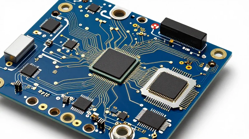
The Architecture of a Secure Biometric PCB
A high-security biometric PCB functions as the central nervous system of a smart lock, requiring a specialized integration of hardware security modules (HSM), high-speed processing, and sensitive analog-to-digital sensor interfaces. To maintain system integrity, the PCB must isolate the biometric acquisition circuitry from the primary application processor, ensuring that raw fingerprint or facial data is encrypted locally before being transmitted to the secure element.
Core Components and Their Roles
| Component | Primary Function | High-Security Requirement |
|---|---|---|
| Microcontroller (MCU) | Instruction execution and I/O management | Must feature Arm TrustZone or similar TEE |
| Secure Element (SE) | Cryptographic key storage | Tamper-evident hardware with physical shielding |
| Power Management IC (PMIC) | Regulated voltage distribution | Low-quiescent current for battery longevity |
| Sensor Interface | Data acquisition from scanner | SPI/I2C encryption support |
Key Design Considerations
- What role does the Secure Element play in biometric storage?
The Secure Element acts as a vault for biometric templates, ensuring that sensitive data is stored in a physically isolated environment that is inaccessible via standard debugging interfaces. - How does power management impact security?
Robust power management prevents brownout attacks and ensures that the system maintains enough voltage to complete cryptographic operations during unexpected power instability. - Why is trace routing critical for biometric PCBs?
Proper trace routing prevents signal crosstalk and electromagnetic interference (EMI), which could otherwise leak biometric data patterns that are susceptible to eavesdropping.
Biometric Sensor Integration and Signal Integrity

Optimizing Signal Paths for Biometric Accuracy
The bridge between a biometric sensor and the microcontroller (MCU) is the most critical path in your PCB design. To achieve low False Rejection Rates (FRR), you must treat the transmission line as a high-speed signal path. Even minor electromagnetic interference (EMI) or impedance mismatches can corrupt raw biometric data, leading to failed reads or increased latency as the system repeatedly requests sensor re-scans.
Interface Selection: SPI vs. I2C vs. MIPI
| Interface Type | Throughput Speed | Signal Integrity Risk | Best Use Case |
|---|---|---|---|
| I2C | Low | Moderate | Capacitive wake-up triggers |
| SPI | High | Low | Main fingerprint image transfer |
| MIPI-CSI | Very High | Critical | High-resolution facial recognition |
Mitigating Noise and Latency
High-security locks often operate in noise-prone environments with proximity to door motors and wireless radios. Implementing a clean power supply chain—specifically using dedicated low-dropout regulators (LDOs) for the biometric module—prevents switching noise from the lock's actuator from injecting artifacts into the sensor's analog-to-digital converter.
- How do I prevent motor noise from affecting sensor readings?
Utilize physical isolation on the PCB layout and implement dedicated power filtering stages (ferrite beads and decoupling capacitors) for the biometric front-end. - Does trace length significantly impact authentication latency?
Yes. Keep traces as short as possible and match their lengths to minimize signal skew. Excessive length increases capacitance, which slows down high-speed SPI/MIPI clock signals. - What role does shielding play in security?
Proper shielding prevents 'side-channel' signal leakage. High-security PCBs should use ground planes surrounding sensitive analog traces to ensure the integrity of the biometric capture.
Prioritizing Hardware Ruggedness for Extreme Environments
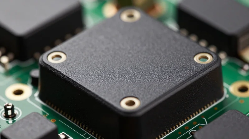
Designing for Environmental Resilience
Biometric PCBs deployed in external or industrial settings must survive thermal cycling and moisture ingress that would otherwise cause rapid component degradation. Ruggedness is not merely a choice of casing but starts at the board level with conformal coating, vibration-resistant mounting, and industrial-grade components designed to operate beyond the standard consumer temperature range of 0°C to 70°C.
| Environmental Factor | PCB Mitigation Strategy | Expected Benefit |
|---|---|---|
| Temperature Extremes | AEC-Q100 Grade Components | Maintains stable clock frequency and sensor accuracy. |
| High Humidity | Silicone/Acrylic Conformal Coating | Prevents dendritic growth and shorts on sensitive traces. |
| Physical Vibration | Underfill and Rigid-Flex Support | Protects solder joints from fatigue and micro-fractures. |
Fortifying Against Physical Tampering
In high-security applications, the PCB must act as its own first line of defense. Selecting a board design that incorporates physical security measures—such as active mesh layers, tamper-responsive sensors, and hardened enclosures—is critical to preventing side-channel attacks and physical extraction of biometric data.
- How does moisture impact sensor accuracy?
Humidity causes electrolytic corrosion on unprotected traces, leading to signal degradation and potential false triggers or system failure in biometric sensors. - Why are standard consumer-grade components insufficient?
Consumer components lack the thermal tolerance and humidity resistance required for outdoor environments, leading to drift in biometric authentication accuracy over time. - What is the role of conformal coating?
Conformal coating provides a thin, protective dielectric layer that shields PCB components from humidity, salt spray, and particulate contaminants.
Encryption and Secure Element Implementation
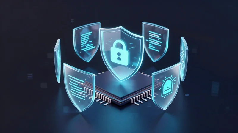
The Role of Secure Elements in Biometric Integrity
A standard microcontroller unit (MCU) is insufficient for storing sensitive biometric data. For high-security smart door locks, a dedicated Secure Element (SE) is non-negotiable. The SE acts as a hardware-based vault, isolating cryptographic keys and biometric templates from the primary system processor. By performing sensitive operations within an environment resistant to side-channel attacks and physical probing, the SE ensures that even if the primary PCB is compromised, the master biometric credentials remain inaccessible.
Encryption Standards for Biometric Data
To prevent credential theft, data must be encrypted both at rest and in transit. Using AES-256 for local storage and ECC (Elliptic Curve Cryptography) for secure key exchange provides a robust defense against intercept and replay attacks. The PCB design must ensure that the communication bus between the biometric sensor and the Secure Element uses encrypted data lines to prevent 'man-in-the-middle' injections.
| Security Feature | Implementation Strategy | Primary Defense |
|---|---|---|
| Hardware Isolation | Dedicated Secure Element | Physical tampering/Side-channel |
| Data at Rest | AES-256 Bit Encryption | Extraction of stored templates |
| Data in Transit | Encrypted Bus (I2C/SPI) | Eavesdropping/Replay attacks |
Security Implementation FAQ
- Why can't I just use the MCU's internal Flash memory?
Standard MCU memory lacks the tamper-detection mechanisms and physical security hardening of an SE. It is susceptible to diagnostic port extraction and voltage glitching attacks. - Does encryption increase latency in the lock release process?
Minimal. While encryption adds computational overhead, modern Secure Elements perform cryptographic operations in milliseconds, which is negligible compared to the physical mechanical latency of the lock strike. - How is the Secure Element updated?
Updates are handled via secure bootloaders using authenticated cryptographic signatures, ensuring that only manufacturer-signed firmware can ever be loaded onto the device.
Power Efficiency and Battery Lifecycle Management
Achieving an ideal balance between high-security biometric processing and battery longevity requires an architectural approach that prioritizes deep-sleep efficiency, optimized power rail design, and event-driven wake-up logic.
Implementing Efficient Power States
The PCB must be designed to remain in a near-zero power state while awaiting user interaction. By utilizing an ultra-low-power microcontroller (MCU) that supports wake-up on GPIO interrupt, the system avoids high-drain polling. The primary goal is to isolate high-current components—such as the optical or capacitive sensor modules and the Secure Element—from the power rail unless they are actively required for authentication.
Component Selection for Low-Power Profiles
| Component Class | Power Management Priority | Key Optimization Metric |
|---|---|---|
| MCU/Processor | High | Nano-amp sleep current |
| Biometric Sensor | Critical | Fast wake-up time (<200ms) |
| Secure Element | Medium | Low quiescent current consumption |
| DC-DC Converters | High | Efficiency at light loads |
Battery Lifecycle Management Strategies
- How does intelligent voltage regulation extend battery life?
Using high-efficiency switching regulators instead of linear regulators reduces heat dissipation and minimizes energy loss, effectively squeezing more usable capacity out of lithium or alkaline battery sets. - Why is sensor wake-up speed important for battery longevity?
A sensor that requires a long duration to boot and initialize increases the 'active' time of the system, draining significant current. Selecting components with rapid wake-up capabilities ensures the system returns to deep-sleep immediately following a scan. - What role do load switches play in power isolation?
Load switches allow the system to physically disconnect power from non-critical peripheral circuits when not in use, preventing 'leakage current' that often drains smart lock batteries prematurely.
Navigating Global Certification Standards
Achieving global market viability for high-security biometric smart door locks requires navigating a complex matrix of regulatory compliance and performance-based security certifications. When selecting a PCB for these systems, developers must prioritize compliance early in the design cycle to avoid costly hardware revisions that could jeopardize certification timelines.
Essential Regulatory Compliance Standards
Regulatory standards are mandatory legal requirements for market entry, focusing on electromagnetic compatibility (EMC), radio frequency (RF) safety, and electrical performance. Failure to comply can result in product seizure or significant legal penalties.
| Standard | Region | Primary Focus |
|---|---|---|
| FCC Part 15 | USA | Electromagnetic interference and RF emissions for digital devices. |
| CE Marking | EU | Health, safety, and environmental protection requirements. |
| UL 294 | USA | Access control system unit safety and physical security testing. |
| RoHS/REACH | Global | Restriction of hazardous substances in electronic components. |
Security and Durability Certifications
Beyond basic legal requirements, industry-specific security certifications demonstrate that your PCB can withstand sophisticated physical and digital attack vectors. These certifications serve as the hallmark of trust for high-security residential and commercial applications.
- BHMA (Builders Hardware Manufacturers Association)
Certifies the physical robustness and mechanical security of the lock assembly; high grades indicate superior cycle life and resistance to forced entry. - FIPS 140-2/3
The benchmark for cryptographic modules; essential if your PCB handles biometric templates and encryption keys in government or enterprise-level settings. - EN 14846
The European standard for electromechanically operated locks, defining performance requirements for reliability and security against physical tampering.
Best Practices for Compliance-Driven PCB Design
To streamline the certification path, PCB design must incorporate 'compliance-by-design' methodologies. This includes utilizing pre-certified RF modules to simplify FCC/CE wireless certification, implementing trace isolation to meet strict EMC emissions standards, and choosing components with verified safety ratings for fire and electrical surge protection.
Evaluating Supplier Reliability and Quality Assurance

Selecting the right manufacturing partner for high-security biometric PCBs extends beyond simple cost-per-unit analysis. Because smart locks are exposed to varying environmental conditions and constant physical interaction, your PCB must meet stringent reliability benchmarks. Vetting a supplier requires a deep dive into their fabrication tolerances, component sourcing transparency, and adherence to rigorous quality management systems like ISO 9001 and IATF 16949.
Key Metrics for Supplier Quality Evaluation
| Evaluation Criterion | Benchmark Requirement | Risk of Failure |
|---|---|---|
| ISO/IATF Compliance | ISO 9001:2015 | High process variation |
| Component Sourcing | Authorized distributors only | Counterfeit part insertion |
| Inspection Process | AOI and X-ray testing | Hidden soldering defects |
| Environmental Stress | HALT testing capabilities | Premature field failure |
Supply Chain Resilience and Longevity
High-security smart locks often have a product lifespan exceeding five years. Ensuring long-term availability of sensitive components—such as secure elements or specific fingerprint sensor controllers—is paramount. You must demand a formal obsolescence management policy from your manufacturer to avoid costly redesigns caused by sudden component EOL (End-of-Life) notices.
Frequently Asked Questions on Quality Assurance
- How do I verify the authenticity of components?
Require a full bill of materials (BOM) traceability report and certificates of conformance (CoC) from authorized original component manufacturers (OCMs). - Why is Automated Optical Inspection (AOI) insufficient for high-security PCBs?
AOI cannot detect internal layer shorts or BGA (Ball Grid Array) solder joint fractures. You should mandate AXI (Automated X-ray Inspection) for any board utilizing dense ICs. - What indicates a manufacturer is 'high-security' ready?
They should demonstrate experience with IPC-A-610 Class 3 standards, which are reserved for mission-critical hardware where failure results in significant security breaches.
Selecting the right biometric PCB is the cornerstone of building a trusted smart lock system. By prioritizing signal integrity, hardware resilience, and strict compliance, you safeguard your brand's reputation and your customers' peace of mind. Ready to refine your hardware strategy? Contact our engineering team today to discuss your smart lock project requirements and ensure your design is ready for the market.
