
The demand for portable power has never been higher, but the physical limitations of legacy Silicon-based PCBA designs are hitting a wall. As consumers demand faster charging in smaller form factors, engineers must pivot to Gallium Nitride (GaN). This guide explores why the transition to GaN is no longer optional for companies aiming to lead the market.
The Evolution of Power Electronics: From Silicon to GaN
The Silicon Era: Reaching Theoretical Limits
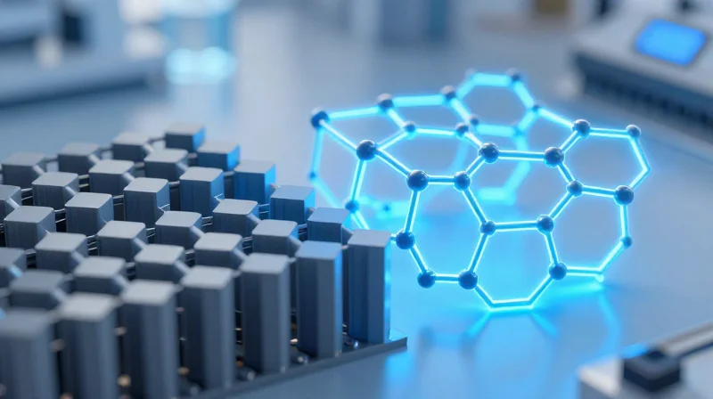
For decades, Silicon (Si) has served as the backbone of the semiconductor industry. Its dominance was driven by cost-effectiveness, mature manufacturing processes, and reliable performance in moderate power applications. However, as demands for higher power density and faster switching frequencies grew in portable electronics, silicon began hitting its physical ceiling. Because silicon has a relatively narrow bandgap (1.1 eV), it experiences higher energy losses as heat when pushed to operate at higher voltages and frequencies, limiting the miniaturization potential of charger PCBAs.
The Rise of Wide Bandgap (WBG) Semiconductors
The industry breakthrough arrived with Wide Bandgap (WBG) materials, specifically Gallium Nitride (GaN). Unlike silicon, GaN features a significantly wider bandgap (3.4 eV), which allows it to withstand higher electric fields and operate at higher temperatures without losing its semiconducting properties. This fundamental material shift enables engineers to design chargers that are significantly smaller, lighter, and more efficient than their silicon predecessors.
| Feature | Silicon (Si) | Gallium Nitride (GaN) |
|---|---|---|
| Bandgap Energy | 1.1 eV | 3.4 eV |
| Switching Frequency | Low | Very High |
| Thermal Conductivity | Moderate | Superior |
| Size/Form Factor | Bulky | Compact |
Understanding the GaN Advantage
- Why does bandgap matter in charging?
A wider bandgap allows electrons to move more freely while resisting breakdown at higher voltages, resulting in lower power loss during switching cycles. - How does GaN reduce charger size?
Because GaN switches more efficiently at higher frequencies, the passive components like transformers and capacitors can be significantly smaller, drastically reducing the total PCBA footprint. - Is silicon obsolete?
Not entirely; while GaN is superior for high-density fast charging, silicon remains cost-effective for low-power, high-volume consumer applications where extreme miniaturization is not the primary requirement.
Understanding the Physics: Why GaN Outperforms Silicon
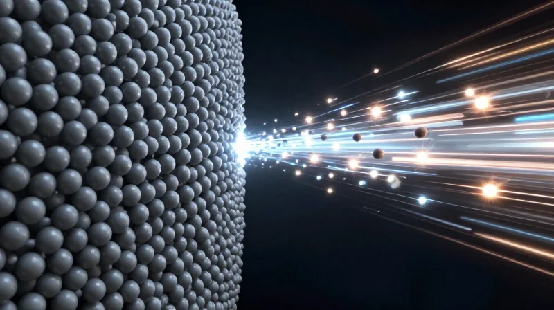
The primary performance gap between silicon (Si) and Gallium Nitride (GaN) lies in their atomic-level physical properties. While silicon has been the industry standard for decades, it is reaching its physical limits in terms of power density and switching efficiency. GaN, a wide-bandgap (WBG) semiconductor, changes the power conversion landscape by allowing electrons to move more freely and enabling the handling of higher voltages without the energy loss typical of silicon-based transistors.
The Advantage of Wide Bandgap and Electron Mobility
A material's bandgap determines how much energy is required to excite an electron from the valence band to the conduction band. Silicon possesses a bandgap of 1.1 eV, whereas GaN boasts 3.4 eV. This wider gap allows GaN devices to operate at significantly higher temperatures and voltages. Furthermore, GaN offers much higher electron mobility compared to silicon, which reduces 'on-resistance.' This reduction in resistance is critical because it minimizes power dissipation as heat, allowing for vastly improved efficiency during the rapid switching cycles required in modern fast-charging protocols.
Technical Comparison: Si vs. GaN Performance
| Feature | Silicon (Si) | Gallium Nitride (GaN) |
|---|---|---|
| Bandgap (eV) | 1.1 | 3.4 |
| Electron Mobility | Moderate | High |
| Switching Frequency | Lower | Very High |
| Heat Dissipation | Higher Loss | Lower Loss |
Common Inquiries Regarding GaN Physics
- Why does higher switching frequency matter?
Higher switching frequencies allow engineers to use significantly smaller passive components, such as inductors and transformers, drastically reducing the overall physical footprint of the PCBA. - Does GaN eliminate heat generation entirely?
No material can eliminate heat, but GaN's superior efficiency significantly lowers power loss during operation, which translates to cooler devices and less demand for large, bulky heat sinks. - Why has silicon been used for so long if GaN is better?
Silicon manufacturing processes are highly mature and inexpensive; the adoption of GaN is a relatively recent shift driven by the urgent market demand for smaller, more efficient portable power solutions.
Efficiency Gains and Heat Dissipation Benefits
The primary advantage of GaN technology in power electronics lies in its superior energy conversion efficiency and thermal conductivity. By utilizing a Wide Bandgap (WBG) structure, GaN devices achieve significantly lower conduction and switching losses. This reduction in wasted energy, which manifests primarily as heat, allows for smaller, more efficient printed circuit board assemblies (PCBAs) that do not require bulky heat sinks.
Efficiency Gains: Minimizing Power Loss
In traditional silicon MOSFETs, energy is lost during the rapid switching cycles necessary for fast charging, primarily due to parasitic capacitance and switching delay. GaN transistors exhibit much lower parasitic capacitance and faster switching speeds, which dramatically reduce these energy losses. Consequently, a higher percentage of input energy is converted into usable power for the device, enabling manufacturers to deliver higher wattages in a smaller form factor without exceeding thermal limits.
Thermal Management and Enclosure Design
Efficient power conversion simplifies the thermal management challenge. Because GaN components generate less heat, PCBAs can be designed with higher power densities and tighter component placement. This shift reduces the overall enclosure size, enabling the ultra-compact, portable power adapters increasingly demanded by consumers. Furthermore, the robust nature of GaN allows these materials to operate safely at higher temperatures, reducing the dependency on extensive active or passive cooling mechanisms.
| Parameter | Silicon (Traditional) | Gallium Nitride (GaN) |
|---|---|---|
| Switching Frequency | Low/Moderate | High/Ultra-High |
| Energy Conversion Efficiency | Lower | Higher (up to 95%+) |
| Heat Dissipation | Significant; requires large sinks | Minimal; enables compact designs |
| Component Size | Bulky | Very Compact |
Frequently Asked Questions
- Why does GaN produce less heat?
GaN has lower conduction resistance and lower switching losses compared to silicon, resulting in less energy dissipation as heat during power conversion. - How does GaN affect PCBA size?
Lower heat generation allows for denser component placement and the removal of bulky thermal management hardware, directly enabling smaller, lighter PCBA designs. - Can GaN withstand higher temperatures?
Yes, GaN is a Wide Bandgap semiconductor that maintains its physical properties and performance stability at higher temperatures compared to traditional silicon counterparts.
Shrinking the Footprint: Achieving Smaller PCBA Designs
The High-Frequency Advantage in Component Miniaturization
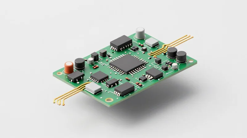
The primary driver of PCB shrinkage in GaN-based chargers is the ability to operate at significantly higher switching frequencies compared to traditional silicon-based MOSFETs. By increasing the frequency, the energy storage requirements for passive components—specifically transformers, inductors, and capacitors—are reduced. As these components scale inversely with frequency, GaN allows engineers to utilize smaller inductive and capacitive elements without sacrificing performance or increasing ripple current.
| Component Type | Silicon Impact (Lower Frequency) | GaN Impact (Higher Frequency) |
|---|---|---|
| Transformer | Large magnetic core required | High flux density allows smaller cores |
| Capacitors | High capacitance needed for filtering | Smaller capacitance suffices |
| Inductors | Bulkier wire-wound components | Integrated or low-profile designs |
Optimizing Board Layout and Thermal Density
Beyond component size, GaN technology facilitates higher power density by streamlining the PCB layout. Because GaN devices exhibit lower parasitic capacitance and inductance, designers can pack components closer together without risking electromagnetic interference (EMI) or unintended parasitic coupling. This reduction in trace length and board real estate creates more room for thermal dissipation strategies, such as smaller heat sinks or even utilizing the PCB copper layers themselves to conduct heat.
Common Questions on GaN Miniaturization
- Why do higher frequencies lead to smaller components?
Passive components like inductors and capacitors are sized based on the energy storage required per cycle; higher frequencies mean each cycle is shorter, necessitating less energy storage and smaller component values. - Does switching faster create more EMI noise?
While faster switching does present design challenges, the improved edge control and lower gate drive requirements of GaN allow for cleaner, faster switching, often simplifying the overall filtering network. - Are there limitations to how small a PCBA can get?
Yes, thermal management and safety clearances (creepage and clearance distances) mandated by regulatory standards provide a physical floor for how much a design can realistically be shrunk.
The Impact on Consumer Experience and Market Competitiveness

Elevating the Consumer Experience
The transition from silicon to GaN is not merely a technical upgrade; it is a shift toward a more seamless mobile lifestyle. For the end-user, this manifests as lighter, slimmer chargers that fit effortlessly into travel bags without sacrificing power. By leveraging GaN’s superior efficiency, manufacturers can produce multi-port adapters that maintain cool surface temperatures, enhancing user safety and product longevity.
Market Competitiveness: GaN vs. Silicon
| Feature | Traditional Silicon | GaN Technology |
|---|---|---|
| Form Factor | Bulky and dense | Compact and lightweight |
| Charging Speed | Moderate/Standard | Ultra-fast/High-density |
| Thermal Output | High | Low |
| Market Position | Legacy/Cost-sensitive | Premium/Performance-driven |
Key Considerations for Consumers
- Does GaN technology cost more for the end user?
While GaN chargers often carry a higher price tag due to semiconductor costs, the long-term value lies in their durability and the versatility of carrying one charger for multiple devices. - Why is aesthetics a competitive factor?
Modern consumer electronics favor minimalist design; GaN allows for cleaner, smaller device silhouettes that were impossible with traditional silicon power systems. - How does this affect market entry for brands?
Brands that adopt GaN technology signal to the market that they prioritize innovation, forcing competitors to pivot away from aging silicon architectures to remain relevant.
Reliability and Longevity in Modern Power Banks
Reliability and Longevity in Modern Power Banks
The transition to GaN technology in portable power raises critical questions regarding structural integrity and wear cycles. Contrary to misconceptions that smaller, high-frequency components might burn out faster, GaN-on-Si power devices exhibit robust field reliability due to their high critical breakdown field strength and improved thermal resilience compared to conventional Silicon MOSFETs.
Durability Under Stress
GaN devices operate at significantly higher temperatures without the degradation of switching performance that often plagues silicon. By minimizing internal resistance, GaN reduces the cumulative thermal stress applied to surrounding capacitors and PCB traces, effectively extending the MTBF (Mean Time Between Failures) of the entire charging module.
| Reliability Metric | Silicon (Si) MOSFET | GaN Power FET |
|---|---|---|
| Thermal Stability | Moderate; prone to runaway at high heat | Excellent; wide bandgap resilience |
| Switching Frequency | Low/Mid; limited by parasitic capacitance | Ultra-High; reduced switching losses |
| Lifespan Expectancy | Standard industry average | High; reduced thermal degradation |
Frequently Asked Questions
- Does the smaller size of GaN power banks sacrifice build quality?
No; GaN allows for higher power density, meaning internal components are subjected to less heat, which actually improves the lifespan of associated passive components like capacitors. - Are GaN transistors prone to early failure?
Modern GaN-on-Si power devices are mature and validated through JEDEC standards, showing reliability levels equivalent to or exceeding traditional silicon components in daily charge/discharge cycles. - How does thermal management improve component life?
Lower operating temperatures prevent the 'baking' of electrolyte in capacitors, which is the primary cause of failure in older portable power designs.
Cost-Benefit Analysis: The ROI of Transitioning Your Product Line
While Gallium Nitride (GaN) components carry a higher unit price than mature silicon MOSFETs, the total cost of ownership and product lifecycle profitability favor GaN. By reducing the physical size of power conversion circuitry, manufacturers can significantly lower costs in housing materials, shipping logistics, and retail packaging, creating a net-positive financial impact that extends beyond simple bill-of-materials (BOM) accounting.
Beyond the BOM: The Economic Multipliers of GaN
| Cost Driver | Silicon-Based Design | GaN-Enabled Design |
|---|---|---|
| Passive Components | Large, bulky, higher quantity | Compact, fewer, reduced count |
| Enclosure Material | High volume, heavy duty | Lower volume, lightweight |
| Logistics/Shipping | Expensive due to size/weight | Cost-effective per unit |
| Market Positioning | Budget-tier/Legacy | Premium/High-margin |
Analyzing Long-Term ROI
Transitioning to GaN is an investment in product differentiation. By achieving higher power density, products move from commoditized, low-margin power supplies into premium, high-demand portable charging solutions. The integration of GaN allows for smaller, more efficient thermal management systems, which reduces the need for expensive cooling architectures, effectively recovering the initial silicon cost premium through manufacturing simplification.
- Does GaN's higher component cost hurt overall margins?
No; while the component cost is higher, the system-level savings achieved through smaller PCBs, fewer required cooling components, and lower shipping costs typically result in higher margins on the final retail product. - How does product size impact shipping logistics?
Smaller product footprints allow for higher pallet density during transit, significantly reducing the cost per unit for international shipping and warehousing. - Is the transition to GaN sustainable for mass-market products?
Yes, as the supply chain for GaN matures and economies of scale take effect, the price gap compared to silicon is closing, making it the standard choice for next-generation portable power.
Future-Proofing: How GaN Fits into the Next Decade of Electronics
The Trajectory Toward Universal Power Integration
As we move further into the 2020s, GaN is transitioning from a premium differentiator to a standard expectation in high-performance power electronics. The core of this transition lies in its ability to support higher switching frequencies, allowing passive components—such as transformers and capacitors—to shrink in size, ultimately facilitating the evolution toward smaller, lighter, and more powerful universal power supplies.
GaN vs. Future Silicon Capabilities
| Feature | Silicon (Si) Limit | GaN Advancement |
|---|---|---|
| Switching Frequency | Low/Moderate | Ultra-High |
| Thermal Efficiency | Heat-Limited | Conductive-Optimized |
| Form Factor | Bulky | Ultra-Compact |
Strategic Outlook: Industry Standards and Sustainability
The adoption of GaN is intrinsically linked to broader sustainability goals. By reducing power waste during AC-to-DC conversion, GaN contributes to lower energy consumption across the global electronic landscape. Moving into the next decade, manufacturers who standardize on GaN will find themselves better positioned to meet increasingly stringent global efficiency regulations, such as the EU's energy-related products directive.
- Will GaN render Silicon obsolete?
Silicon will remain dominant in low-power, low-cost applications, but GaN will capture the market for high-performance and high-density power delivery where efficiency is paramount. - How does GaN support future PCBA design?
Its ability to function at higher frequencies allows for the reduction of passive component sizes, enabling designers to optimize PCB space for additional functionality or further miniaturization. - Is the transition to GaN scalable?
Yes, as semiconductor fabrication capacity expands and yield rates continue to improve, the cost gap between GaN and Silicon is closing, making it a viable long-term strategy for mass-market consumer electronics.
Transitioning to GaN technology is the most effective way to distinguish your power products in a crowded market. By leveraging higher efficiency and reduced physical footprints, you can deliver the premium performance consumers expect. Ready to upgrade your power bank manufacturing? Contact our engineering team today to start your transition to GaN.
