
In the race for faster charging cycles and higher energy density, PCB design is no longer just about logic—it is about managing physics. Engineers now face the dual challenge of shrinking form factors while handling substantial thermal and electrical loads. This guide provides an authoritative roadmap to navigating DFM strategies that ensure your next high-power assembly is as reliable as it is powerful.
Understanding the Physics of High-Power Assemblies
Designing for high-power PCBA demands a departure from standard signal-integrity-focused practices, as the physics of energy dissipation and electron transport dominate the board's structural and electrical health. In high-power systems—such as fast-charging controllers or power inverters—the primary enemy is the coupling of high current density with parasitic resistance, which manifests as localized heating. Unlike low-power signal boards, high-power assemblies require a holistic understanding of how board materials, copper geometry, and thermal paths interact to prevent catastrophic failure modes like delamination, trace burnout, or thermal runaway.
Current Density and Joule Heating
At the heart of high-power design is the I²R loss (Joule heating). As current flows through conductors, resistance produces heat directly proportional to the square of the current. In DFM, this necessitates precise calculation of trace cross-sectional areas. Standard design rules often underestimate the cumulative thermal strain placed on the FR-4 dielectric when large components operate at peak thermal loads for extended periods.
| Parameter | Signal-Oriented Design | High-Power DFM |
|---|---|---|
| Copper Thickness | Standard (0.5oz - 1oz) | Heavy (2oz - 4oz+) |
| Thermal Focus | Crosstalk/EMI | Temperature Rise/CTE |
| Via Usage | Signal routing | Thermal dissipation paths |
Material Science Constraints
The Coefficient of Thermal Expansion (CTE) mismatch between copper and the resin-based substrate is a critical failure point. High-power designs induce cyclic thermal expansion that can crack vias or cause micro-fractures in the copper plating. Designers must prioritize substrates with high Glass Transition Temperatures (Tg) and high Decomposition Temperatures (Td) to maintain structural integrity under persistent thermal stress.
Common High-Power Design Challenges
- Why do standard trace widths fail in high-power applications?
Standard widths lack the required cross-sectional area to carry high current without exceeding a 10°C or 20°C temperature rise, leading to rapid degradation of the dielectric material. - How do thermal vias assist in heat regulation?
Thermal vias act as heat pipes, lowering the thermal resistance path between the component junction and the board's internal ground planes or external heat sinks. - What is the role of the Glass Transition Temperature (Tg)?
Tg is the threshold at which the PCB substrate transitions from a rigid state to a softer, rubbery state; exceeding this significantly increases CTE, risking board delamination.
Material Selection for High-Current Conductivity
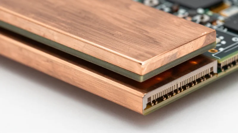
In high-power PCBA designs, standard FR-4 often fails to manage the heat generated by rapid electron flow and extreme current densities. Effective material selection requires a strategic balance between copper thickness, dielectric glass transition temperature (Tg), and thermal conductivity to ensure structural integrity and signal reliability.
Optimizing Copper Weights for Current Capacity
Choosing the appropriate copper weight is the primary defense against resistive heating. Engineers must calculate the cross-sectional area required to keep temperature rise within specified limits, typically referencing IPC-2152 standards.
| Copper Weight | Typical Thickness (mm) | Primary Application |
|---|---|---|
| 1 oz | 0.035 | Standard logic and signal layers |
| 2 oz | 0.070 | Moderate power rails and DC/DC converters |
| 3 oz+ | 0.105+ | Extreme high-current charging circuits |
Dielectric Selection and Thermal Management
Material selection extends beyond copper to the resin system. For high-power boards, high-Tg (Glass Transition Temperature) materials are mandatory to prevent delamination when operating at elevated temperatures. Materials with a Tg above 170°C are generally recommended for fast-charging applications where thermal cycling is frequent.
Frequently Asked Questions
- Why is thermal conductivity critical for high-current traces?
High-current traces generate significant I²R losses; materials with high thermal conductivity help dissipate this heat into the internal copper planes or heat sinks, preventing localized hot spots. - When should I consider using heavy copper boards?
Heavy copper (above 2 oz) is necessary when trace widths are physically constrained by board size but the circuit demands minimal voltage drop and low thermal output under high current. - Does the dielectric material impact dielectric breakdown?
Yes, high-power circuits require substrates with high Comparative Tracking Index (CTI) ratings to resist the formation of conductive paths across the insulator during high-voltage or thermal stress events.
Advanced PCB Layout Techniques for Current Flow
Strategic Copper Distribution and Impedance Minimization
To handle the high current demands of modern fast-charging protocols, designers must shift from signal-integrity-focused routing to power-distribution-centric design. Minimizing resistive losses (I²R) begins with maximizing copper cross-sections; this means utilizing heavier copper weights (2oz to 4oz) and prioritizing wide, short traces that follow the shortest return path to minimize loop inductance.
| Feature | Design Rule | Purpose |
|---|---|---|
| Trace Width | Calculated via IPC-2221 | Prevent conductor overheating |
| Copper Pour | Solid Plane/Pour | Improve thermal mass & lower resistance |
| Via Stitching | Multi-via arrays | Reduce thermal and electrical impedance |
Thermal Regulation Through Advanced Via Arrays
Localized hotspots often stem from insufficient thermal dissipation paths. Integrating thermal via stitching directly under high-power components—such as MOSFETs and GaN switches—allows heat to migrate efficiently to internal ground planes or the bottom side of the PCB. Ensure these vias are not only electrically connected but also thermally conductive by utilizing copper-filled or plated-over-via technology to prevent solder wicking issues during assembly.
Best Practices and FAQs
- Should I use thermal relief pads on high-current connections?
No. Thermal reliefs increase electrical resistance and create a bottleneck for high current. Use solid connections for all high-power pins to ensure maximum contact area. - How does PCB thickness influence high-power design?
A thicker board increases the thermal mass of the system and allows for more robust mechanical support for heavy components, though routing high-current traces on internal layers requires careful planning for heat dissipation. - Can I use standard signal vias for high-current paths?
Generally, no. Standard signal vias are insufficient for high current; you must calculate the total current capacity and utilize an array of multiple parallel vias to distribute the thermal load.
Thermal Management and Heat Dissipation Strategies
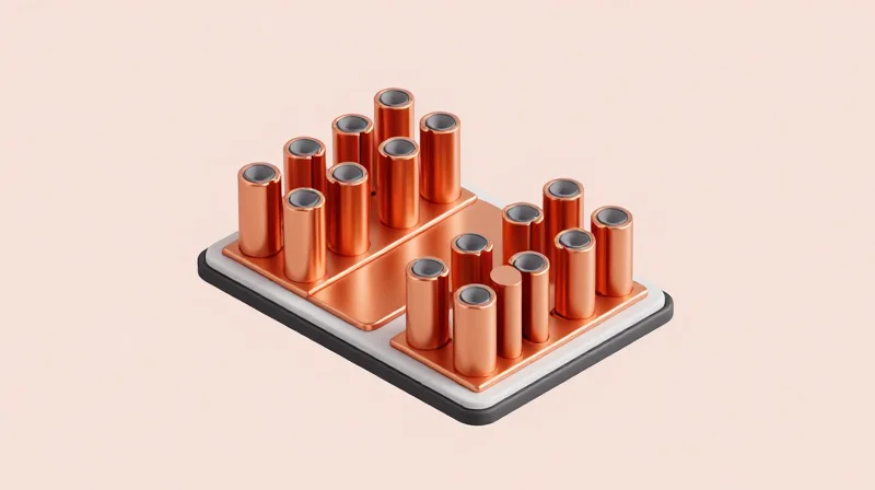
Thermal Management and Heat Dissipation Strategies
In high-power PCBA design, thermal management is not an afterthought but a foundational requirement. Effective heat dissipation in fast-charging circuits relies on lowering thermal resistance (Rθ) between power components and the ambient environment, ensuring that high current densities do not cause localized overheating or dielectric degradation.
Thermal Vias and Copper Plane Integration
Thermal vias act as vertical heat pipes, connecting surface-mounted power components to internal copper ground planes or external heatsinks. For optimal performance, these vias should be filled and capped to ensure high thermal conductivity and to prevent solder wicking during assembly.
| Via Type | Thermal Benefit | Implementation Note |
|---|---|---|
| Standard Plated | Moderate | Risk of solder wicking |
| Filled and Capped | High | Best for high-power density |
| Metal Inlay | Extreme | Expensive; used for direct component contact |
Strategic Component Placement
Segregating high-heat generating components—such as MOSFETs, transformers, and inductors—is critical. Place these devices near board edges to facilitate better convective cooling, and avoid placing temperature-sensitive ICs in the immediate thermal shadow of high-current paths.
Frequently Asked Questions
- How many thermal vias are necessary for a power MOSFET?
While there is no fixed number, aim for a tight grid under the thermal pad. Increasing via diameter beyond 0.3mm often yields diminishing returns; instead, increase the count of smaller, high-density vias to maximize surface area. - Does a thicker copper weight improve thermal performance?
Yes. Increasing copper weight from 1oz to 2oz or 3oz significantly reduces lateral thermal resistance, allowing heat to spread more efficiently across the PCB substrate before dissipation. - Should heatsinks be soldered or bolted?
For high-vibration environments, bolted heatsinks with thermal interface material (TIM) are preferred. If using soldered heatsinks, ensure the assembly process accounts for the thermal mass of the heatsink to prevent cold solder joints.
Minimizing Impedance for Signal and Power Integrity
Minimizing Parasitic Inductance and Resistance
Achieving signal and power integrity in high-power PCBA requires a rigorous approach to controlling parasitic elements. High-frequency charging circuits and fast-switching power stages are highly sensitive to loop inductance; therefore, minimizing the return path area is the most effective strategy to prevent electromagnetic interference and voltage spikes.
| Design Parameter | Impedance Mitigation Effect | Key DFM Best Practice |
|---|---|---|
| Copper Thickness | Reduces DC Resistance | Use 2oz+ copper for power planes |
| Via Stitching | Lowers Loop Inductance | Place ground vias near signal exits |
| Stack-up Design | Reduces Mutual Inductance | Use thin prepreg for tight coupling |
Key Strategies for Power and Signal Integrity
- How does plane proximity impact impedance?
Placing power and ground planes on adjacent layers with minimal dielectric thickness increases inter-plane capacitance, which stabilizes high-frequency voltage rails and lowers characteristic impedance. - What is the role of decoupling capacitors?
Strategically placing low-ESR (Equivalent Series Resistance) ceramic capacitors as close as possible to the IC power pins minimizes the current loop path, effectively shunting transient noise before it impacts signal integrity. - How should high-speed differential pairs be routed?
Maintain constant trace geometry and ensure that high-speed signals have a continuous reference plane beneath them to prevent impedance discontinuities that lead to reflections.
Advanced Via Management
Vias act as small inductors in high-power systems. To mitigate this, design engineers should employ back-drilling to remove non-functional via stubs in high-speed nets. For power delivery networks, utilize multiple vias in parallel to distribute current density, which reduces total resistance and minimizes localized thermal impedance that could otherwise cause board-level fatigue.
DFM Strategies to Meet International Safety Standards
Aligning DFM with Global Regulatory Frameworks
To achieve international compliance for high-power PCBA designs, DFM must transition from being a process optimization tool to a safety-centric methodology. Designers must prioritize creepage and clearance distances, material flammability ratings, and thermal isolation during the initial layout phase to avoid costly late-stage redesigns necessitated by safety testing failures.
| Standard | Focus Area | DFM Implementation Strategy |
|---|---|---|
| UL 94 | Material Flammability | Specify V-0 rated FR-4 and solder mask materials. |
| IEC 60950/62368 | Creepage and Clearance | Enforce strict keep-out zones for primary-to-secondary isolation. |
| IPC-2152 | Current-Carrying Capacity | Use IPC-compliant trace width calculations considering temperature rise. |
Essential Compliance Checklist
- How do I ensure adequate isolation in high-power layouts?
Apply mandatory spacing rules defined in IEC 62368-1 based on the working voltage, considering both peak voltage and environmental pollution degrees. - Which IPC standard governs current-carrying capacity?
IPC-2152 is the gold standard for determining conductor widths, replacing older, conservative IPC-2221 guidelines to prevent overheating under load. - Why is material selection critical for DFM?
Safety standards require specific Thermal Index (TI) and Comparative Tracking Index (CTI) ratings for PCB substrates to ensure long-term arc resistance and fire safety.
Proactive DFM is not just about manufacturability; it is about establishing a design margin that satisfies global inspectors. By automating design rule checks (DRC) for creepage and clearance, teams can eliminate human error during the layout of high-voltage fast-charging circuitry.
Prototyping and Simulation: Predicting Real-World Performance
The Role of Digital Twin Simulation
Modern high-power PCBA development relies on creating a 'digital twin' of the circuit, where electrical and thermal stressors are modeled simultaneously. By simulating current distribution and heat dissipation under extreme fast-charging loads, designers can identify potential hotspots, current crowding, or dielectric stress points that would otherwise lead to failure in physical prototypes.
Key Simulation Methodologies
| Simulation Type | Primary Goal | Critical Metric |
|---|---|---|
| FEA Thermal Analysis | Predict component operating temps | Junction temperature (Tj) |
| DC IR Drop Analysis | Identify voltage drops and power loss | Current density (A/mm²) |
| CFD Airflow Simulation | Optimize enclosure/heatsink cooling | Nusselt number/Velocity |
Bridging Simulation to Physical Prototyping
Simulation is not a replacement for physical testing but a filter to ensure the first hardware iteration is functional. Once simulations confirm thermal equilibrium, physical prototypes should be subjected to 'burn-in' tests using infrared thermography to correlate real-world values with predicted data points. This feedback loop ensures that future simulation models remain accurate as design complexity scales.
- Why is thermal simulation critical for fast charging?
Fast charging introduces high peak currents that can cause localized heating; simulation prevents unexpected board warping or component degradation due to sustained high temperatures. - How do I handle discrepancies between simulation and reality?
Check your thermal conductivity models and material properties; often, discrepancies arise from incorrect PCB stack-up definitions or overly optimistic cooling assumptions. - When is the right time to simulate?
Simulation should start at the layout phase, specifically after finalizing the stack-up and power delivery network (PDN), to catch design flaws while changes are inexpensive.
Quality Assurance and Testing for Reliability
Essential Inspection Protocols for High-Power Reliability
For high-power PCBAs, standard visual inspection is insufficient; manufacturers must employ multi-stage diagnostic testing to ensure that thermal management structures and high-current traces are robust under continuous load.
| Testing Method | Target Failure Point | Reliability Impact |
|---|---|---|
| AOI (Automated Optical Inspection) | Solder bridging and component alignment | Prevents short circuits during high-voltage operation |
| X-Ray (AXI) | BGA voids and internal layer shorts | Ensures thermal pad connectivity for heat dissipation |
| Micro-Sectioning | Plated-through-hole (PTH) integrity | Validates copper plating thickness for high current capacity |
Advanced Testing Procedures for Fast Charging Performance
Validating the performance of fast charging circuits requires hardware-in-the-loop (HIL) testing to simulate transient response and thermal cycling. Stress testing should replicate extreme ambient conditions to detect early signs of component degradation due to Joule heating.
- How does thermal cycling affect long-term PCBA reliability?
Rapid transitions between ambient and operating temperatures cause mechanical stress on solder joints, particularly in high-power zones, which can lead to fatigue fractures if coefficient of thermal expansion (CTE) mismatches are not addressed. - Why is impedance testing critical for high-power traces?
Accurate impedance control in power paths minimizes parasitic inductance, which prevents voltage spikes and electromagnetic interference during rapid current switching in fast-charging applications. - What role does thermal imaging play in QA?
Infrared thermography is used during board-level power-up testing to identify localized 'hot spots' that indicate poor thermal interface material application or inadequate copper pouring.
Successfully designing high-power PCBA requires a perfect synergy between thermal engineering and precise layout execution. By prioritizing DFM early in the development cycle, you can mitigate risks and accelerate time-to-market. Ready to optimize your hardware? Contact our engineering team today for a comprehensive design review of your next project.
