
In the fast-paced world of industrial edge computing, the failure of a single circuit board can lead to catastrophic downtime. Choosing the right HDI PCB manufacturer is not just a sourcing decision; it is a critical engineering partnership that determines whether your gateway survives in harsh, mission-critical environments.
The Critical Role of HDI in Industrial Edge Computing
The Necessity of HDI in Modern Edge Gateways
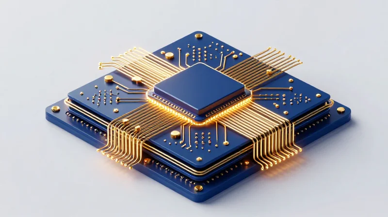
Industrial edge computing gateways must process vast amounts of sensor data with minimal latency while remaining compact enough to deploy in space-constrained factory environments. HDI technology facilitates this by utilizing laser-drilled microvias, finer lines, and tighter spaces compared to traditional multi-layer PCBs. This high-density routing capability allows designers to integrate complex System-on-Chips (SoCs), high-speed FPGAs, and dense memory architectures into a significantly smaller footprint without compromising signal integrity or thermal management.
HDI vs. Traditional PCB Technology for Industrial Applications
| Metric | Traditional PCB | HDI PCB |
|---|---|---|
| Via Structure | Through-hole | Microvia (Blind/Buried) |
| Component Density | Low to Moderate | High |
| Signal Integrity | Limited at high speeds | Excellent (reduced trace length) |
| Form Factor | Bulkier | Compact/Miniaturized |
Strategic Advantages of HDI
- Signal Integrity Optimization
By reducing the length of interconnects and minimizing parasitic capacitance, HDI design ensures cleaner signal transitions for high-frequency data transmission. - Thermal Management Efficiency
Advanced HDI layering allows for better integration of thermal vias and ground planes, critical for dissipating heat in high-performance computing chipsets. - Space and Weight Reduction
Minimizing board surface area allows for smaller overall device enclosures, a primary requirement for deployment in rugged industrial field locations.
Evaluating Material Reliability and Thermal Performance

Understanding Key Thermal Parameters
For industrial edge gateways, the reliability of the PCB substrate is paramount. You must prioritize materials that offer specific thermal thresholds to prevent delamination, pad lifting, and conductive anodic filament (CAF) formation under fluctuating operational loads.
| Parameter | Significance | Industrial Standard Target |
|---|---|---|
| Glass Transition Temperature (Tg) | Temperature at which material changes from rigid to soft. | Greater than 170°C |
| Decomposition Temperature (Td) | Temperature at which the material chemically degrades. | Greater than 340°C |
| Coefficient of Thermal Expansion (CTE) | Rate of material expansion during heat cycles. | Low Z-axis CTE (<3%) |
Evaluating Material Reliability
When vetting a manufacturer, demand documentation on their material selection processes. High-performance gateways often experience rapid thermal cycling; therefore, matching the CTE of the dielectric material to that of copper is essential to prevent via-barrel cracking in HDI structures.
- Why is Tg critical for edge gateways?
Edge gateways generate significant heat in compact enclosures; a high Tg ensures the PCB maintains structural integrity and electrical consistency well above standard ambient temperatures. - How does Td impact long-term reliability?
A higher Td provides a safety buffer during the reflow soldering process and continuous high-load operations, preventing long-term material breakdown and loss of insulation resistance. - What is the consequence of mismatched CTE?
Mismatched CTE leads to excessive Z-axis expansion during thermal cycling, which places immense mechanical stress on small-diameter microvias, often resulting in premature field failures.
Adherence to IPC Standards as a Quality Benchmark
The Non-Negotiable Standard for Industrial HDI PCBs
For industrial edge computing gateways, where failure is not an option, IPC compliance serves as the universal language of quality and manufacturing excellence. While many manufacturers claim capability, only those strictly adhering to IPC-A-600 (Acceptability of Printed Boards) and IPC-6012 (Qualification and Performance Specification for Rigid Printed Boards) can guarantee the structural integrity required for complex HDI designs.
Key IPC Benchmarks for Mission-Critical Hardware
| IPC Standard | Primary Focus | Industrial Impact |
|---|---|---|
| IPC-A-600 | Visual Acceptance | Identifies defects like plating voids or misregistration early. |
| IPC-6012 | Performance Testing | Ensures thermal cycling and vibration resistance for harsh environments. |
| IPC-CC-830 | Conformal Coating | Critical for moisture and contaminant protection in edge gateways. |
Why IPC Certification Dictates Reliability
- Mitigation of Micro-Via Failure
Strict adherence to IPC-6012 Class 3 requirements ensures that the complex micro-via structures inherent in HDI designs are subjected to rigorous cross-section analysis, preventing latent failures. - Consistency in Material Integrity
IPC standards mandate specific testing for thermal shock and coefficient of thermal expansion (CTE) matching, ensuring the PCB does not delaminate during rapid temperature swings. - Supply Chain Traceability
Certified manufacturers maintain comprehensive documentation of every production run, allowing for precise forensic analysis if a field failure occurs.
When vetting a partner, verify their specific certification status against IPC-6012, specifically focusing on Class 3 requirements, which are mandatory for high-reliability industrial and medical applications. A manufacturer operating without these documented benchmarks is essentially guessing at the longevity of your edge gateway.
Assessing Technical Capabilities and Manufacturing Capacity

For industrial edge computing, manufacturing capacity is defined by more than raw throughput; it is measured by the capability to execute complex HDI designs with high yield. Manufacturers must demonstrate mastery over laser drilling for micro-vias, reliable via-in-pad (VIPPO) processes, and the thermal management required for high-frequency signal integrity.
Critical Manufacturing Capabilities for HDI
| Feature | Technical Requirement | Impact on Performance |
|---|---|---|
| Laser Drilling | Blind/Buried micro-vias < 100μm | High-density routing and reduced crosstalk |
| Via-in-Pad | Conductive epoxy filling and planarization | Improved signal integrity and component density |
| Surface Finish | ENIG or ENEPIG | Corrosion resistance and superior solder joint reliability |
Key Considerations for Process Verification
- How do you verify laser drilling precision?
Request cross-sectional analysis reports to ensure that laser ablation is clean with minimal heat-affected zones, preventing delamination and ensuring copper plating adhesion. - Why is copper plating uniformity critical for HDI?
In high-performance edge gateways, inconsistent plating thickness in micro-vias leads to impedance discontinuities and thermal expansion stress points, which are common failure modes in industrial environments. - What should be expected from a manufacturer's Quality Management System?
The manufacturer should provide documented statistical process control (SPC) data specifically for HDI features, including via registration accuracy and plating thickness distribution across the entire panel.
Ultimately, the right partner for high-performance edge computing will not only offer advanced technical specifications but also provide transparency regarding their scaling capability. Ensure they can maintain high yields during prototype-to-production transitions, as process drift in micro-via formation can drastically impact the reliability of your final gateway deployment.
The Importance of Design for Manufacturing (DFM) Feedback
The Strategic Value of Early DFM Engagement
For industrial edge computing gateways, where HDI (High-Density Interconnect) designs involve complex blind and buried vias, thin cores, and high-frequency requirements, DFM is not just a review process—it is a critical engineering partnership. A manufacturer that offers DFM feedback *before* the design is finalized can identify potential failure points such as aspect ratio violations in microvias, inadequate solder mask dams, or impedance mismatches that arise from non-optimal copper balancing.
DFM Impact on Product Lifecycle
| Parameter | Without Early DFM | With Proactive DFM |
|---|---|---|
| Design Iterations | Multiple cycles to fix board fails | Optimized in first pass |
| Cost Impact | High rework and scrap rates | Reduced material waste |
| Time to Market | Delayed due to manufacturing holds | Accelerated validation |
Frequently Asked Questions regarding DFM
- Why is DFM critical for HDI designs?
HDI designs push the physical limits of PCB fabrication. Without DFM, designs often exceed the laser drill capabilities or plating throw-ratios of the factory, leading to reliability issues in the field. - How does early DFM reduce long-term costs?
By identifying potential issues before board fabrication begins, you avoid expensive tooling revisions, material scrap, and the engineering overhead associated with redesigning complex high-speed stacks. - Should I share my design intent or just the Gerber files?
Sharing your design intent—such as critical high-speed signal paths or thermal dissipation goals—allows the manufacturer to provide more nuanced advice, ensuring that DFM changes do not inadvertently hurt your electrical performance.
Supply Chain Stability and Intellectual Property Security
Securing the Supply Chain for Industrial Edge Hardware
For industrial edge computing, supply chain instability translates directly into deployment failure. You must evaluate a manufacturer not just on their production throughput, but on their sourcing resiliency and geographical risk profile. A robust manufacturer maintains secondary sourcing agreements for high-grade copper laminates and specialty chemicals, ensuring that production remains uninterrupted even during global material shortages.
Intellectual Property (IP) Protection Standards
Your HDI PCB design is the blueprint for your gateway's competitive advantage. Protecting Gerber files, layer stack-up data, and impedance profiles is non-negotiable. Ensure your manufacturer operates under strict NDA frameworks and utilizes secure, encrypted portals for design file transfers. Proactive IP management prevents unauthorized cloning and design leakage.
| Risk Category | Assessment Metric | Best Practice |
|---|---|---|
| Material Sourcing | Secondary Supply Chain | Audit supplier tier-2 material lists |
| Data Handling | Digital Infrastructure | Encryption in transit and at rest |
| IP Integrity | Access Control | Restrict file access by user role |
Frequently Asked Questions
- How do I verify a manufacturer's IP security?
Request a SOC2 Type II compliance audit or evidence of an internal information security management system (ISMS) specifically tailored to manufacturing operations. - What is the danger of offshore HDI production?
Geopolitical volatility and longer lead times introduce significant risk. If choosing offshore, ensure the manufacturer has strong local legal presence and compliance with international trade law. - Does a DFM report compromise my IP?
A reputable firm treats DFM feedback as confidential documentation. The exchange should always occur within a secure environment covered by a Master Services Agreement (MSA) that includes explicit IP protection clauses.
Verifying Quality Control and Testing Protocols

For edge computing gateways, where reliability under thermal stress and high-speed data integrity are non-negotiable, a manufacturer's testing regimen must extend far beyond standard electrical continuity checks. A robust quality protocol relies on the synergy between non-destructive inspection, precise metrology, and deep-layer verification to detect micro-vias and interconnect defects that standard testing often misses.
Essential Inspection and Testing Technologies
| Inspection Method | Primary Application | Key Benefit for HDI |
|---|---|---|
| AOI (Automated Optical Inspection) | Surface trace and solder joint integrity | Rapid detection of surface shorts and alignment errors. |
| Flying Probe Testing | Electrical net verification | Flexible testing for complex, high-density netlists without costly fixtures. |
| X-Ray Inspection | Internal layer alignment and BGA solder | Visualizing buried micro-vias and internal BGA defects. |
Deep-Dive into HDI-Specific Procedures
Manufacturers specializing in HDI must employ specific methodologies to validate high-density interconnects. Automated Optical Inspection (AOI) should be deployed post-lamination to identify trace defects before they are buried. Furthermore, X-ray inspection is critical for boards using 'via-in-pad' technology; it allows quality engineers to verify the alignment and void-free nature of solder connections within high-density BGA packages.
- Does the manufacturer provide detailed test reports?
A high-quality partner will offer comprehensive FA (Failure Analysis) reports, including X-ray images and micro-section analysis, rather than just a simple pass/fail certificate. - How is reliability validated under environmental stress?
Look for HAST (Highly Accelerated Stress Test) or thermal cycling capabilities to ensure the copper integrity of micro-vias holds up under the temperature fluctuations common in edge gateways. - Is the inspection process automated or manual?
Manual inspection is prone to human error; prioritize facilities that use AI-driven AOI systems for consistent detection of trace anomalies.
Finally, ensure that your manufacturer maintains IPC-Class 3 certification standards. While Class 2 is acceptable for general consumer goods, edge computing gateways often operate in extreme conditions that demand the stringent acceptance criteria, inspection depth, and documentation rigor mandated by Class 3 protocols.
Long-Term Scalability and Support Structures
Transitioning from Prototype to Mass Production
The challenges of manufacturing high-performance HDI boards scale non-linearly when moving from a pilot run to mass production. A competent partner must demonstrate proven methodologies for process stabilization, ensuring that the tight tolerances required for laser-drilled microvias and ultra-fine pitch components are maintained across thousands of units rather than just a handful of prototypes.
Operational Maturity and Quality Consistency
| Feature | Prototype Capability | High-Volume Requirement |
|---|---|---|
| Process Control | Manual/Semi-automated | Full Automation with SPC |
| Material Sourcing | Spot Buy | Strategic Partnership/Lock-in |
| Quality Audit | Functional Check | Comprehensive Yield Analysis |
Key Considerations for Long-Term Support
- How does the manufacturer manage material end-of-life (EOL)?
A reliable partner maintains proactive obsolescence management and works with you to re-qualify alternative materials or components before they impact production. - What is their policy on capacity reservation?
For industrial edge projects, confirm the manufacturer has dedicated capacity or tiered priority levels so your production does not get sidelined by larger consumer-electronics orders. - Is there a mechanism for ongoing yield improvement?
Look for manufacturers who conduct post-production DFM refinement to iteratively improve board yield and reduce cost-per-unit over the product lifecycle.
Engineering Support Structures
Long-term success in edge computing hinges on the responsiveness of the manufacturer's engineering team. Beyond simple fabrication, look for partners who offer dedicated account engineers who understand the specific thermal management and signal integrity requirements of your high-performance design. This continuity prevents the need to 're-teach' the design intent to new personnel during the manufacturing cycle.
Choosing the right PCB manufacturer is a strategic investment in the longevity and reliability of your industrial systems. By prioritizing material science, rigorous quality standards, and collaborative DFM support, you can mitigate risk and accelerate your time-to-market. Contact our engineering team today to audit your next project and ensure your edge gateways are built to last.
