
In the world of high-performance electronics, the transition to 10 to 32-layer PCBs introduces exponential challenges in signal integrity, thermal dissipation, and structural reliability. Selecting the wrong partner can lead to catastrophic field failures and costly redesigns. This guide provides an authoritative framework to vet manufacturers capable of handling the most rigorous complex design requirements.
Assessing Technical Capability for High-Layer Counts
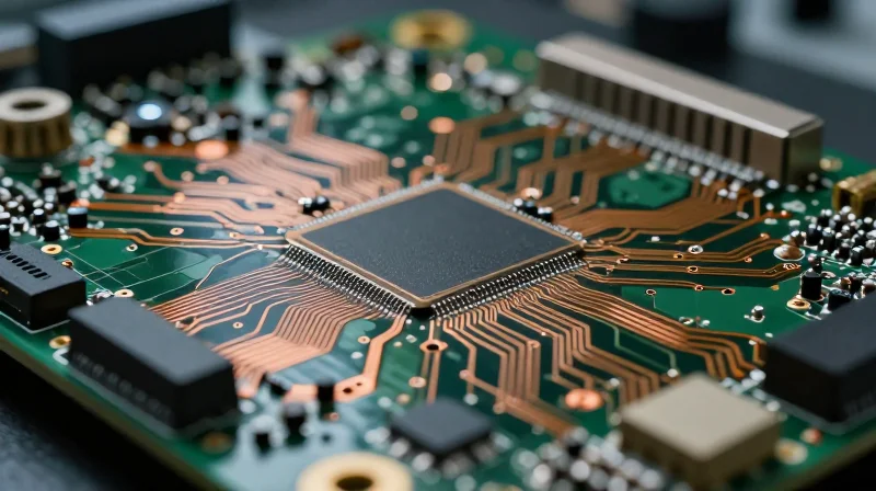
When transitioning to high-layer count designs—typically exceeding 12 layers—the margin for error in registration and thermal stability effectively vanishes. Manufacturers must demonstrate mastery over multi-stage lamination cycles and laser-via drilling precision to maintain signal integrity and structural reliability throughout the production run.
Critical Technical Parameters for High-Density Stacks
| Parameter | Requirement for High-Layer Boards | Impact on Performance |
|---|---|---|
| Layer Registration | Inner-layer accuracy within +/- 1 mil | Prevents impedance mismatches and via-drilling breakthroughs |
| Drill Precision | Aspect ratio control beyond 10:1 | Ensures reliable plating in deep micro-vias |
| Lamination Symmetry | Balanced copper distribution across layers | Mitigates board warpage and mechanical stress |
Registration and Alignment Mastery
The greatest technical challenge in high-layer manufacturing is maintaining registration accuracy across each lamination cycle. As boards grow thicker, material shrinkage and expansion during heat cycles can cause inner-layer features to shift. A capable manufacturer should utilize advanced X-ray registration systems and automated optical alignment (AOI) to compensate for these material distortions dynamically.
Frequently Asked Questions
- How do I verify a manufacturer's lamination capability?
Request documentation on their lamination press capabilities, specifically regarding vacuum-assisted systems that minimize void formation in high-density stacks. - What role does material selection play in high-layer count reliability?
Choosing high-Tg and low-CTE materials is non-negotiable, as these materials better withstand the repetitive thermal stress inherent in complex, high-layer board processing. - Should I require a capability audit?
Yes. A site visit or a virtual audit focusing on their registration equipment and cleanroom environmental controls is essential to validate their technical readiness.
Mandatory Quality Certifications and Industry Standards
Essential Certifications for High-Reliability PCBs
When managing designs with 12 to 30+ layers, quality certifications act as a filter to ensure the manufacturer possesses the robust process controls required to prevent delamination, signal integrity failures, and registration drift.
| Certification | Significance | Application |
|---|---|---|
| ISO 9001 | Foundational Quality Management | Baseline requirement for all professional manufacturing. |
| IPC-6012 Class 3 | High-Reliability Performance | Mandatory for mission-critical and complex high-layer boards. |
| AS9100 | Aerospace/Defense Standards | Ensures strict traceability and risk mitigation. |
| ISO 13485 | Medical Devices | Necessary for life-critical healthcare electronic hardware. |
Why IPC-6012 Class 3 is Non-Negotiable
For complex electronic designs, IPC-6012 Class 3 represents the gold standard. Unlike Class 2, which allows for minor cosmetic or structural imperfections, Class 3 demands absolute compliance regarding annular ring requirements, copper plating thickness in vias, and dielectric spacing. Manufacturers operating at this level have the automated optical inspection (AOI) and X-ray systems necessary to verify these tolerances throughout the production cycle.
Frequently Asked Questions
- Does an ISO certification alone guarantee high-layer capability?
No, ISO 9001 is a management system. You must specifically verify that the manufacturer audits their processes against IPC-6012 Class 3 to ensure they can physically execute high-layer count designs. - How do I verify a manufacturer's claims?
Request their current registration certificates and ask for their latest audit reports or their CAGE code for defense-related projects, which often serves as a secondary validation of their operational standards. - What is the consequence of choosing a provider without these certifications?
You face a high risk of 'latent defects,' where the board passes initial testing but fails in the field due to thermal cycling, vibration, or impedance inconsistencies inherent in poorly processed multi-layer structures.
Thermal Management and Material Expertise

Thermal Management and Material Expertise
For designs reaching 32 layers or more, the density of components and traces creates significant localized heat pockets that standard FR-4 materials cannot withstand. A competent manufacturer must possess deep expertise in managing the Coefficient of Thermal Expansion (CTE) across a heterogeneous stack-up. Selecting the right high-Tg (Glass Transition Temperature) material is critical to preventing delamination and ensuring mechanical stability when the board experiences the rapid thermal cycling typical of complex, high-power electronic systems.
Thermal Dissipation Strategies
Beyond material choice, the manufacturer must demonstrate proficiency in implementing active thermal solutions. This includes precise drilling and copper-filling of thermal vias to move heat efficiently from internal layers to outer planes, as well as the successful integration of metal-core or copper-coin technology to act as a heat sink for power-hungry silicon.
| Thermal Solution | Best Used For | Manufacturing Complexity |
|---|---|---|
| High-Tg Laminates | Preventing delamination | Low |
| Thermal Vias | Internal heat distribution | Medium |
| Copper Coins/Metal Cores | High-wattage components | High |
- How do I verify a partner's material expertise?
Ask for their material library and experience with specific high-speed, high-Tg resin systems like Megtron or ISOLA; request case studies on how they have mitigated CTE mismatch in similar layer counts. - What is the primary risk of neglecting thermal design in 32-layer boards?
The primary risk is micro-via fracture caused by Z-axis expansion during thermal cycling, which leads to intermittent failures that are notoriously difficult to troubleshoot. - Why is copper-filling required for thermal vias?
Copper-filling provides a solid thermal path that is significantly more conductive than standard via plating, ensuring heat does not become trapped within the insulation layers.
Advanced Drilling and Via-in-Pad Capabilities
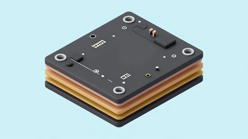
Mastering Microvia and Via-in-Pad Technologies
As component pitch shrinks and pin density increases, traditional through-hole via technology becomes insufficient. Selecting a manufacturer requires verifying their proficiency in microvia formation—typically via laser ablation—and their capability to perform via-in-pad (VIP) plating processes. Reliable VIP implementation requires robust copper-fill processes to ensure structural integrity and prevent surface unevenness that could compromise solder joint reliability.
Comparison of Via Technologies
| Via Type | Fabrication Method | Primary Application | Complexity Level |
|---|---|---|---|
| Through-Hole | Mechanical Drill | General Routing | Low |
| Blind/Buried | Laser/Mechanical | Layer-to-Layer interconnect | Medium |
| Via-in-Pad | Plated & Capped | High-density BGA | High |
Sequential Lamination and Registration Precision
For complex, high-layer count PCBs, sequential lamination is often mandatory. This process involves multiple sub-lamination cycles to create blind or buried vias. A manufacturer's success here depends on their registration accuracy across these cycles. Failure to maintain tight tolerances during lamination can lead to via-to-pad misalignment, causing intermittent opens or shorts that are notoriously difficult to detect during standard automated optical inspection (AOI).
- How do you evaluate a manufacturer's laser drilling capability?
Request data on their laser drill throughput, spot size capabilities (down to 50µm or less), and their ability to handle various dielectric materials without leaving excessive carbonization or 'drill smear' inside the hole. - Why is copper filling of microvias essential?
Copper-filled vias allow for a flat solderable surface directly over the via, which prevents solder wicking, reduces capacitance, and ensures a solid connection for ultra-fine-pitch BGA components. - What should be specified in the fabrication notes regarding alignment?
Clearly define your tolerance requirements for layer-to-layer registration and specify the IPC standards (e.g., IPC-6012 Class 3) that dictate the minimum annular ring requirements for your specific drill-to-pad design.
Signal Integrity and Impedance Control Protocols
Validating Impedance Control Methodologies
For complex, high-layer count designs, maintaining strict impedance control—often within ±5%—is non-negotiable for high-speed signal integrity. A qualified manufacturer must go beyond standard coupons; they should demonstrate mastery over dielectric constant (Dk) consistency, trace geometry precision, and copper foil treatment profiles. During the selection process, prioritize partners who integrate Time Domain Reflectometry (TDR) testing directly into their production workflow rather than treating it as a secondary, batch-sampled task.
Technical Requirements for Signal Integrity
| Requirement | Verification Metric | Industry Standard |
|---|---|---|
| Impedance Tolerance | TDR Coupon Measurement | ±5% or better |
| Signal Loss (Insertion) | VNA S-Parameter Testing | Minimize dielectric dissipation |
| Registration Accuracy | X-Ray Alignment Imaging | IPC Class 3 standards |
Evaluating Manufacturer Software and Simulation Tools
Modern signal integrity is governed by software-driven simulation that predicts performance before the first board is ever etched. Verify that your partner utilizes industry-standard field solvers (such as Polar SI9000 or Ansys HFSS) to analyze stack-up configurations. They should be willing to share their 'impedance calculation model' and collaborate with your design team to adjust trace widths or dielectric thicknesses to account for the actual manufacturing variables specific to their facility.
- How do I ensure the manufacturer's TDR testing is accurate?
Request their TDR report templates and ask for verification of calibration intervals on all testing equipment to ensure adherence to NIST-traceable standards. - Why does the manufacturer need to know my dielectric constant (Dk) expectations?
Materials behave differently at high frequencies; the manufacturer must use the Dk values provided by the resin-coated copper or prepreg supplier to tune their impedance calculations effectively. - Should I require test coupons on every panel?
Yes, for high-density, high-layer count designs, test coupons should be placed on every production panel to provide a statistically significant data set for yield and impedance verification.
Supply Chain Stability and Production Scalability
Ensuring Supply Chain Resilience
For complex high-layer designs, the supply chain is as critical as the engineering specifications. Manufacturers must maintain long-term relationships with laminate suppliers to ensure consistent availability of specialized materials such as high-Tg, low-DK, and low-DF substrates. A lack of upstream inventory management can lead to unexpected material substitutions, which may catastrophically alter the signal integrity or thermal performance of your design.
Production Scalability: Prototyping vs. Full-Rate Production
A common failure point in complex electronics is selecting a fabricator that excels at quick-turn prototyping but lacks the industrial footprint for full-rate production. Scalability requires identical process controls across different manufacturing lines, ensuring that the impedance values achieved in a 5-board prototype remain identical in a 5,000-board production run.
| Feature | Prototyping Focus | Volume Production Focus |
|---|---|---|
| Material Sourcing | High availability/Fast transit | Contracted supply/Price hedging |
| Tooling | Soft tooling/Low cost | Hard tooling/High efficiency |
| Process Validation | Functional testing | Automated Optical/X-ray Inspection |
| Capacity Management | Agile floor scheduling | Dedicated production lines |
Strategic Assessment FAQ
- How do I verify a manufacturer's material stability?
Request a certificate of origin for base materials and ask for their material turnover rate to ensure they are not using outdated or shelf-expired laminates. - Does the manufacturer use the same line for prototypes and production?
Ideally, they should have dedicated lines. If the prototype runs on a specialized NPI (New Product Introduction) line, ensure that the manufacturing parameters are strictly transferable to the mass production facility. - What indicators suggest a manufacturer is struggling with scale?
Look for high lead-time volatility, frequent requests for material deviations, and a lack of standardized automated testing protocols across their floor.
The Role of DFM (Design for Manufacturing) Support

Bridging the Gap Between Design and Fabrication
For complex high-layer count designs, the transition from CAD files to physical board production is fraught with potential failure points. Engaging your manufacturer early in the design cycle allows their engineering team to conduct a comprehensive DFM review, identifying issues such as insufficient clearance, stack-up imbalances, or non-manufacturable trace geometries before they become costly production setbacks.
Strategic Advantages of DFM Integration
Proactive DFM feedback significantly shortens time-to-market by eliminating the iterative 'ping-pong' cycles between design and manufacturing. When a manufacturer provides actionable DFM reports, they essentially act as an extension of your internal engineering department, ensuring that the design intent is fully compatible with their specific fabrication capabilities.
| DFM Focus Area | Risk Mitigation Strategy | Project Impact |
|---|---|---|
| Stack-up Symmetry | Ensure uniform copper distribution | Prevents board warping |
| Aspect Ratio | Optimize hole size vs. board thickness | Increases plating reliability |
| Via Placement | Check drill-to-copper margins | Reduces internal shorts |
Common DFM Questions for Prospective Partners
- How early in the design process can we submit files for review?
A high-quality partner will offer design review services during the preliminary layout stage to catch major errors early. - What specific software platforms are used for DFM analysis?
Look for manufacturers using advanced tools like Valor or similar industry-standard CAM software to ensure accuracy. - Does the DFM support include impedance modeling consultation?
Yes, top-tier partners will verify your stack-up against their own material libraries to ensure impedance targets are met.
Verification of Quality Assurance and Inspection Systems

Advanced Inspection Protocols for Multilayer Reliability
For designs exceeding 12 or 16 layers, traditional testing methods are insufficient. You must demand evidence of high-resolution Automated Optical Inspection (AOI) integrated into both inner-layer processing and post-reflow assembly. Furthermore, X-ray inspection is non-negotiable for blind and buried via verification, ensuring that the internal registration maintains structural and electrical continuity throughout the stack-up.
| Inspection Technology | Primary Application | Critical Benefit |
|---|---|---|
| In-process AOI | Inner-layer circuit patterns | Pre-lamination defect detection |
| 2D/3D X-Ray | Blind/Buried Via registration | Void identification in solder joints |
| Micro-sectioning | Cross-sectional stack-up | Verification of copper thickness/plating |
Verifying Quality Assurance Standards
- Does the manufacturer provide 3D AOI or 2D?
3D AOI is essential for identifying lift-off components and solder volume issues that 2D systems often miss, particularly in high-density BGA packages. - What is the frequency of X-ray inspection in your production flow?
A high-end manufacturer should conduct X-ray inspection as a standard process for all multilayer boards, not just as a spot check or upon specific customer request. - Can they demonstrate adherence to IPC Class 3 standards?
For mission-critical designs, the manufacturer must provide objective evidence, such as Cpk reports for registration accuracy and documentation of void percentages, proving they meet the strict IPC-A-600 Class 3 requirements.
Finally, assess their commitment to data transparency. A qualified partner should be willing to share inspection reports, including the specific software versioning and calibration dates of their diagnostic equipment, ensuring that the data you review is accurate and actionable.
Selecting a partner for high-layer count PCBs is a strategic decision that impacts the total lifecycle cost and performance of your product. By focusing on certified processes and proven thermal management expertise, you mitigate risk and ensure long-term reliability. Are you ready to optimize your supply chain? Contact our engineering team today to discuss your next complex PCB project.
