
In the fast-evolving landscape of the Industrial Internet of Things (IIoT), the reliability of your data infrastructure hinges on the gateway. Whether you are monitoring remote assets or managing a smart factory floor, the PCB architecture you choose serves as the foundation for your connectivity. This guide cuts through the technical noise to help you build resilient, scalable LoRaWAN gateways that stand the test of time and environment.
Defining the Industrial Requirement: Beyond Consumer Grade
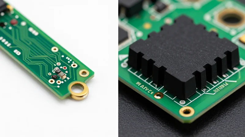
The Failure Threshold of Consumer-Grade Hardware
Consumer-grade PCBs are engineered for controlled indoor environments with predictable thermal cycles and limited electromagnetic interference. When deployed in industrial settings, these components suffer from accelerated fatigue, signal degradation, and failure under constant vibration. An industrial-grade LoRaWAN gateway PCB must be designed for 24/7 uptime, necessitating a shift from standard surface-mount components to high-reliability, ruggedized alternatives capable of enduring extreme temperature fluctuations and electrical noise.
Comparative Analysis: Consumer vs. Industrial Standards
| Feature | Consumer-Grade | Industrial-Grade |
|---|---|---|
| Temperature Range | 0°C to 40°C | -40°C to +85°C |
| Vibration/Shock | Standard/Low | High-G Rating/Resistant |
| EMI Protection | Minimal | Multi-layer Grounding/Shielded |
| PCB Material | Standard FR-4 | High-Tg FR-4 / Ceramic |
Core Reliability Requirements
- Thermal Stability
Industrial PCBs require materials with a high Glass Transition temperature (Tg) to prevent delamination during prolonged heat exposure in factory environments. - Signal Integrity in Noisy Environments
Robust LoRaWAN connectivity requires aggressive EMI shielding and optimized trace impedance to prevent packet loss in environments saturated with heavy machinery and electrical noise. - Scalability and Lifecycle
Unlike consumer electronics which have short revision cycles, industrial PCBs must guarantee component availability for 5-10 years to prevent costly system redesigns.
Environmental Hardening: Thermal and Physical Considerations
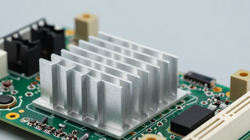
Substrate and Thermal Management
Industrial LoRaWAN gateways are often deployed in unconditioned enclosures where ambient temperatures swing drastically. To prevent delamination and solder joint fatigue, high-Tg (glass transition temperature) FR-4 substrates are mandatory. Materials with a Tg above 170°C offer superior dimensional stability compared to standard consumer-grade boards, ensuring the PCB does not warp or crack under constant thermal cycling.
| Material Feature | Industrial Standard | Benefit |
|---|---|---|
| Glass Transition (Tg) | > 170°C | Prevents thermal warping and board delamination. |
| CTE (Z-axis) | Low (<3.0%) | Reduces stress on plated through-holes during cycling. |
| Surface Finish | ENIG or Hard Gold | Improves corrosion resistance and solder joint integrity. |
Mitigating Vibration and Moisture
Physical durability is achieved through both board-level reinforcement and chemical protection. High-vibration industrial settings necessitate heavy-copper traces and non-conductive mechanical support pillars for heavy components. Furthermore, to combat humidity and potential condensation in outdoor LoRaWAN deployments, applying a silicone-based conformal coating is a critical final assembly step.
- Why is conformal coating necessary for LoRaWAN gateways?
Gateway PCBs are prone to oxidation and short-circuits caused by airborne pollutants and condensation; a thin, non-conductive polymer layer seals the circuitry from moisture ingress. - How do we handle thermal expansion for high-power components?
Use thermal vias and copper pours connected to internal ground planes to distribute heat, supplemented by thermal interface materials (TIM) that bridge the gap between the component and the chassis. - What is the role of heavy-copper in physical stability?
Heavy-copper (typically 2oz or higher) not only handles higher current for RF power amplifiers but also adds mechanical stiffness to the PCB, reducing the likelihood of fatigue-related cracking under vibration.
Power Budget Optimization for Long-Range Deployment
Power Budget Optimization for Long-Range Deployment
Achieving sustainable energy autonomy in industrial LoRaWAN gateways requires a rigorous approach to power distribution. By minimizing quiescent current and optimizing the power path, engineers can extend deployment lifespans significantly, even in environments where solar harvesting is intermittent or battery replacement is cost-prohibitive.
High-Efficiency Power Path Design
The foundation of a successful power budget is the selection of ultra-low IQ (quiescent current) voltage regulators. Standard linear regulators are generally insufficient due to significant energy waste as heat. Instead, prioritize synchronous buck converters that maintain high conversion efficiency even at light load conditions. Incorporating load switches allows for the complete power-gating of non-essential sensors or communication modules during sleep cycles, effectively reducing the baseline current to the micro-ampere range.
| Power Management Strategy | Primary Benefit | Implementation Tip |
|---|---|---|
| Dynamic Voltage Scaling | Reduces active power consumption | Lower CPU clock when idle |
| Load Gating | Eliminates leakage currents | Use high-side MOSFET switches |
| Supercapacitor Buffering | Handles peak pulse currents | Reduces battery voltage sag |
Energy Harvesting Considerations
For solar-powered gateways, the PCB must feature an efficient Maximum Power Point Tracking (MPPT) circuit to extract the maximum available energy from the solar panels. The power management integrated circuit (PMIC) should be selected for its ability to handle wide input voltage ranges and offer integrated battery charging profiles suited for LiFePO4 or Lithium-Ion chemistries, which are preferred for their cycle life in industrial temperature ranges.
- How does PCB trace resistance affect power efficiency?
Long, thin traces increase parasitic resistance, leading to I2R power losses. Ensure wide power planes for high-current paths to minimize voltage drop and energy loss. - Why should I avoid standard electrolytic capacitors?
In outdoor industrial settings, electrolytic capacitors suffer from high ESR increases and electrolyte drying at extreme temperatures, causing unstable power rails; use tantalum or ceramic capacitors instead. - Can I use software to manage the power budget?
Yes, implementing deep sleep states in your firmware and disabling unused peripheral clocks or GPIO pull-ups is just as critical as the physical PCB design.
RF Signal Integrity and LoRaWAN Performance
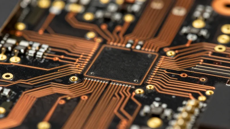
Minimizing Signal Loss in Industrial RF Paths
In industrial LoRaWAN gateways, even minor signal attenuation can lead to significant range degradation and packet loss. Achieving optimal performance requires a strictly controlled 50-ohm impedance environment from the radio transceiver output to the antenna connector. Designers must minimize the electrical length of transmission lines and prioritize high-frequency, low-loss laminate materials like PTFE or specialized hydrocarbon ceramics to mitigate dielectric losses at 868/915 MHz frequencies.
Layout Strategies for Antenna Efficiency
| Design Factor | Industrial Best Practice | Impact |
|---|---|---|
| Trace Routing | Minimize length/use coplanar waveguide | Reduces insertion loss |
| Ground Planes | Solid copper pours with via stitching | Prevents EMI/Crosstalk |
| Component Placement | Keep RF path isolated from high-speed digital | Reduces noise coupling |
Frequently Asked Questions: RF Integrity
- How does PCB substrate impact LoRa signal strength?
Standard FR-4 exhibits high dielectric loss at sub-GHz frequencies. Using high-frequency laminates with a stable dielectric constant (Dk) ensures consistent impedance, which is critical for long-range link budgets. - Why is via stitching essential near the RF trace?
Via stitching creates a Faraday cage effect for transmission lines, ensuring a low-inductance ground return path and preventing high-frequency noise from radiating into other layers. - What is the primary cause of poor gateway sensitivity?
Often, it is mismatched impedance at the RF front-end, leading to high Voltage Standing Wave Ratio (VSWR), causing significant signal reflection back into the radio circuitry.
Mitigating Electromagnetic Interference (EMI)
Industrial environments are saturated with EMI from heavy machinery, motors, and lighting ballasts. To maintain LoRaWAN signal integrity, gateways must feature robust shielding over the RF front-end (RFFE) components. Physical compartmentalization on the PCB using metallic surface-mount shields effectively prevents local noise injection from microcontrollers and switching power supplies, ensuring that the sensitive LoRa receiver maintains its specified signal-to-noise ratio.
Navigating Regulatory Compliance Standards
For industrial LoRaWAN gateway PCBs, regulatory compliance is not merely a legal hurdle but a fundamental requirement for reliable performance and interoperability. Selecting components that carry pre-existing certifications significantly reduces the risk of field failure and the financial burden of redundant testing phases.
Essential Regulatory Certification Checklist
| Certification/Standard | Target Market | Critical Focus Area |
|---|---|---|
| FCC Part 15 | North America | Unintentional radiator emissions and RF spectrum usage. |
| CE Marking (RED) | European Union | Radio Equipment Directive compliance for health, safety, and EM compatibility. |
| LoRaWAN Certified | Global | Network interoperability and adherence to official LoRa Alliance protocols. |
| RoHS/REACH | Global | Environmental safety and hazardous material substance control. |
Frequently Asked Questions on Compliance
- Why is 'LoRaWAN Certified' different from hardware certification?
Hardware certification (FCC/CE) confirms your device behaves as a safe radio transmitter, whereas LoRaWAN certification verifies that the device stack adheres strictly to the LoRa Alliance MAC layer specifications for network interoperability. - How does PCB layout impact EMC testing?
Poor signal return paths, insufficient ground planes, and lack of adequate decoupling capacitors increase radiated emissions, which often leads to failure in Electromagnetic Compatibility (EMC) testing rooms. - Can I bypass certification if I use a pre-certified RF module?
Using a pre-certified module streamlines the process, but you must strictly adhere to the module manufacturer's design guidelines, including antenna type and PCB trace length, to avoid needing a full re-certification.
To maintain scalable connectivity, designers should mandate documentation from component suppliers, specifically requesting test reports for electromagnetic interference (EMI). Integrating these findings early into the PCB layout process prevents costly board spins caused by non-compliance during the final validation stages.
Scalability through Modular PCB Architecture
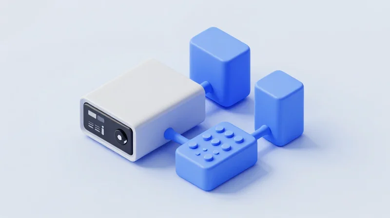
The Benefits of Modular PCB Design for IoT Scalability
In industrial environments where connectivity demands shift rapidly, a monolithic PCB design creates a bottleneck. Modular architecture shifts the paradigm by separating the core processing unit from specialized radio front-ends and I/O interfaces. By utilizing high-density board-to-board connectors or standardized mezzanine slots, engineers can replace radio modules as new LoRaWAN frequency bands or higher-gain hardware become available without discarding the base application processor board.
Comparison of Monolithic vs. Modular Gateway Approaches
| Feature | Monolithic Architecture | Modular Architecture |
|---|---|---|
| Upgradability | Low (Requires full redesign) | High (Component-level updates) |
| Development Speed | Slow (Complex validation) | Fast (Isolated testing) |
| Initial Cost | Lower | Higher |
| Lifecycle Cost | High (Replace entire unit) | Low (Update specific modules) |
Key Strategies for Implementing Modularity
To achieve effective modularity, your PCB design must adhere to strict interface standards. Use standard buses like SPI, I2C, or UART for communication between the processor and radio modules to ensure cross-compatibility. Furthermore, decoupling the power management section ensures that voltage requirements for new, higher-performance modules can be met without re-engineering the primary power distribution network.
- How do board-to-board connectors impact RF integrity?
While convenient, high-speed connectors can introduce impedance discontinuities; it is essential to use shielded connectors and ensure short signal paths to maintain RF signal integrity. - Can I mix and match different radio modules on one baseboard?
Yes, provided the baseboard software driver architecture supports dynamic module discovery, allowing the system to identify and configure different LoRaWAN transceivers automatically. - Does modular design complicate FCC certification?
Using pre-certified RF modules within a modular gateway design can significantly simplify the certification process, as you may only need to perform end-product emission testing rather than full radio testing.
Component Sourcing and Lifecycle Management
The Risk of Component Obsolescence
In industrial IoT, the hardware lifecycle often spans five to ten years. Selecting components with short manufacturing runs creates a high risk of forced redesigns. To maintain scalable connectivity, designers must prioritize components with long-term availability commitments (LTA) and verify the product change notification (PCN) history of every critical integrated circuit, particularly for microcontrollers and transceivers.
Key Strategies for Component Lifecycle Planning
- Prioritize Long-Term Availability
Select silicon providers that explicitly guarantee industrial-grade longevity (typically 10+ years) to avoid disruptive supply chain cycles. - Avoid 'Design-In' Traps
Steer clear of bleeding-edge or niche components that lack a secondary sourcing strategy; always identify drop-in replacements for critical power and RF chips. - Monitor PCN Notifications
Implement a proactive monitoring process to track Product Change Notifications (PCN) and End-of-Life (EOL) announcements from your Tier-1 component suppliers.
Sourcing Strategy Comparison
| Sourcing Strategy | Risk Level | Scalability Impact |
|---|---|---|
| Single-Source Niche | Very High | Critical failure risk |
| Tier-1 Industrial LTA | Low | High reliability |
| Modular/Generic | Minimal | Easy to upgrade |
Effective lifecycle management moves beyond simple sourcing—it involves creating a bill of materials (BOM) that is resilient to regional market volatility. By standardizing on globally available, industry-standard footprints for passives and power management ICs, you ensure that your LoRaWAN gateway remains maintainable even when specific manufacturer stock fluctuates.
Testing and Validation Protocols for Industrial Reliability
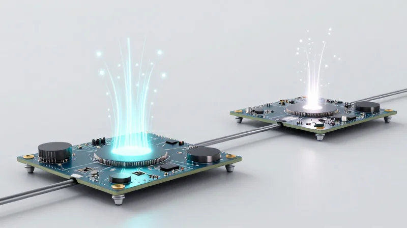
Establishing a Robust Validation Framework
To guarantee long-term operational stability, every LoRaWAN gateway PCB must undergo a multi-stage validation process. This framework moves beyond functional verification, focusing on mechanical integrity, signal performance under noise, and extreme thermal resilience.
Key Stress Testing Protocols
| Test Category | Objective | Industrial Standard |
|---|---|---|
| EMI/EMC Compatibility | Prevent interference in noisy RF environments | CISPR 32 / EN 55032 |
| Accelerated Life Testing (ALT) | Predict MTBF through thermal cycling | JESD22-A104 |
| Vibration/Shock | Ensure solder joint integrity | MIL-STD-810G |
Advanced Testing Procedures Explained
Electromagnetic Interference (EMI) testing is critical for gateways deployed near heavy machinery. By utilizing an anechoic chamber, engineers can identify PCB layout deficiencies—such as insufficient ground planes or poorly routed high-speed traces—that would otherwise compromise sensitive LoRa transceivers. Furthermore, Accelerated Life Testing (ALT) exposes components to extreme thermal swings, forcing early infant mortality failures to occur during the QA phase rather than in the field.
FAQ: Validating Industrial Performance
- Why is ALT critical for gateway PCBs?
ALT simulates years of environmental degradation in days, ensuring that the PCB substrate and solder connections do not develop microscopic fractures due to thermal expansion. - How does EMI testing impact LoRaWAN range?
High levels of internal board noise elevate the noise floor, directly reducing the Link Budget. Strict EMI mitigation ensures the gateway achieves its theoretical maximum sensitivity. - What is the role of Burn-in testing?
Burn-in testing operates the gateway at maximum power consumption for 24-48 hours to identify weak components that fail under prolonged electrical stress.
Selecting the right PCB architecture for your LoRaWAN gateway is the most critical decision in your IIoT development lifecycle. By focusing on environmental ruggedness, power efficiency, and strict regulatory adherence, you ensure your infrastructure provides long-term value. Ready to elevate your hardware strategy? Contact our engineering team today for a consultation on your next industrial gateway project.
