
For hardware engineers, the difference between a prototype that works and a product that scales often lies in the fabrication floor. When your design relies on precise impedance control, choosing the wrong manufacturing partner can lead to catastrophic signal degradation and costly redesign cycles. This guide provides the vetting framework you need to identify a high-end fabrication partner capable of turning your high-speed designs into reliable reality.
The Critical Importance of Impedance Control in PCB Design

In the realm of advanced PCB fabrication, impedance control is not merely a design specification; it is the fundamental governing factor for signal integrity. As signal speeds increase, traces cease to act as simple copper wires and transition into transmission lines. Failure to maintain a consistent characteristic impedance results in signal reflections, ringing, and data corruption, which can render even the most sophisticated digital hardware unreliable.
The Geometric Determinants of Impedance
The characteristic impedance of a signal path is defined by a delicate balance of physical geometry and material properties. Achieving a target impedance, such as 50 ohms single-ended or 100 ohms differential, requires precise control over three primary variables:
- Trace Width and Thickness
The copper geometry determines the inductive and capacitive properties of the trace. Minor deviations caused by etching tolerances can lead to significant impedance discontinuities. - Dielectric Constant (Dk)
The substrate material's Dk defines the speed of the signal and its coupling capacity. Fabricators must ensure consistent resin content and stable material grades to prevent impedance drift. - Dielectric Height
The vertical distance between the trace and the reference plane (prepreg/core thickness) is perhaps the most sensitive factor. Even a slight variation in stack-up thickness drastically alters the return path efficiency.
Impact of Fabrication Variations
| Parameter | Fabrication Variance | Effect on Signal |
|---|---|---|
| Copper Etching | Under/Over Etch | Alters trace width, leading to impedance mismatch. |
| Prepreg Thickness | Resin Flow Variability | Changes height to plane, causing signal reflections. |
| Surface Finish | Electroless Nickel/Gold | Can impact high-frequency skin effect and impedance. |
Because these variables are tightly coupled, advanced designs necessitate a manufacturer who integrates Time Domain Reflectometry (TDR) testing directly into their production workflow. Without rigorous control over the fabrication process, the intended signal integrity—and by extension, the reliability of the entire high-speed system—cannot be guaranteed.
Assessing Dielectric Material Consistency and Inventory
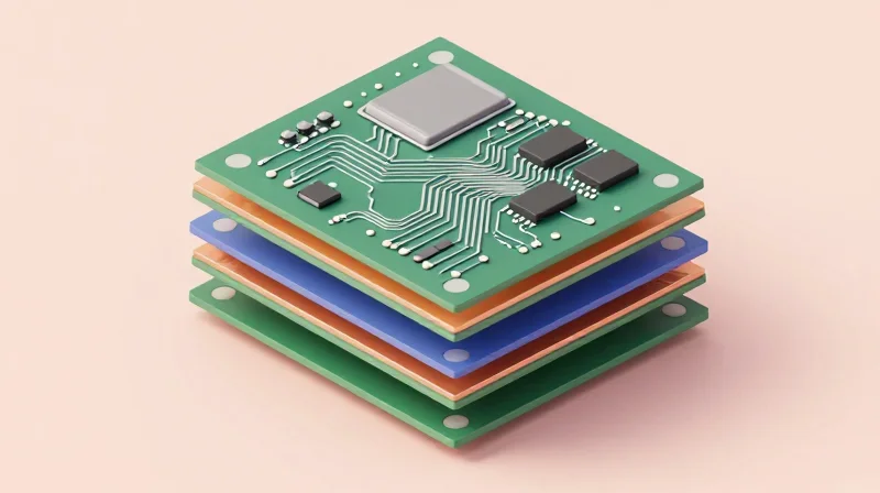
The Impact of Dielectric Variation on Signal Integrity
For advanced impedance controlled projects, the dielectric constant (Dk) is a primary variable. Even subtle shifts in the resin content, glass weave styles, or batch-to-batch variations in laminate materials can lead to significant impedance fluctuations. A manufacturer lacking strict control over its raw material supply chain risks producing boards that fail to meet strict tolerance specifications, leading to signal reflections, electromagnetic interference (EMI), and ultimately, device failure.
Vendor Inventory Management Strategies
| Strategy | Benefit to Impedance Control | Risk if Absent |
|---|---|---|
| Single-Source Procurement | Ensures consistent material properties and Dk values. | Unpredictable shifts in dielectric performance. |
| Batch Tracking | Allows for granular adjustments during etching/lamination. | Difficulty in troubleshooting root cause of impedance drifts. |
| Storage Environmental Control | Prevents moisture absorption which alters effective Dk. | Inconsistent board performance due to humidity fluctuations. |
Critical Questions for Manufacturer Audits
- Do you perform incoming material inspection for dielectric constant?
A high-end manufacturer should verify the Dk of incoming laminates against their supplier certificates rather than relying solely on manufacturer data sheets. - How do you manage cross-batch consistency for long-term projects?
Look for manufacturers who reserve specific laminate lots for a client's project to eliminate variability across different production runs. - Can you provide impedance test data for current material stocks?
A capable partner will offer Coupon Test Reports (TDR) that confirm the material performs as specified under your design constraints.
Evaluating Copper Weight Accuracy and Etching Capabilities
The Impact of Copper Weight on Trace Cross-Sections
Copper weight directly influences the height (thickness) of your traces. In impedance-controlled designs, a 1/2 oz copper layer may behave significantly differently than a 1 oz layer due to the etching process. A manufacturer must be capable of providing precise finished copper thickness data, accounting for the chemical plating and etching reduction factors that occur during production.
Understanding Etch Factor and Trace Geometry
Because chemical etching is an isotropic process, the etchant acts both downward and sideways, creating trapezoidal trace profiles rather than perfect rectangles. The 'etch factor'—the ratio of the trace height to the width of the undercut—is a critical parameter. A reliable manufacturer uses controlled etching parameters to ensure the side-wall angle remains consistent, preventing the impedance from deviating from your calculated design goals.
| Copper Weight | Typical Etch Factor | Impedance Impact |
|---|---|---|
| 0.5 oz | High (3:1 to 4:1) | Less variation; sharper side-walls. |
| 1.0 oz | Moderate (2:1 to 3:1) | Higher risk of trapezoidal profile affecting impedance. |
| 2.0 oz | Low (1:1 to 2:1) | Significant undercut potential requires geometry compensation. |
Questions to Ask Your Manufacturer
- How do you calculate trace compensation?
A qualified manufacturer should automatically adjust your Gerber trace widths to compensate for the anticipated etch loss based on the specific copper weight used. - Do you perform cross-section analysis?
Ask if they routinely use micro-sectioning to verify that the trapezoidal angle matches the impedance model provided during the design phase. - How is plating uniformity managed across the panel?
Uniform current density during electrolytic plating is required to ensure that copper weight is consistent across the entire board surface, not just at the edges.
Understanding Industry-Standard Manufacturing Tolerances
For advanced impedance-controlled projects, manufacturing tolerances are not merely suggestions; they are the governing constraints that determine whether your high-speed signals will function as simulated or fail due to reflection and crosstalk. A competent manufacturer must align their internal process capabilities with recognized standards such as IPC-2141 and IPC-6012, while providing transparent data on their specific operational windows.
Defining Tolerance Ranges for Impedance Control
The industry standard for impedance-controlled traces typically mandates a tolerance of +/- 10%, though highly critical designs often demand +/- 5%. Achieving these tighter windows requires precise control over the PCB fabrication process, including photo-tooling compensation for etching, laminate thickness uniformity, and consistent dielectric constant (Dk) across the board surface.
| Tolerance Class | Typical Application | Fabrication Difficulty |
|---|---|---|
| +/- 10% | Standard High-Speed Digital | Moderate |
| +/- 7% | Advanced Networking/RF | High |
| +/- 5% | Precision High-Frequency/SerDes | Extreme |
Manufacturer Validation and Process Window
When selecting a partner, you must evaluate their ability to provide measurable validation. This includes TDR (Time Domain Reflectometry) coupons tested on every production panel. A manufacturer should be capable of providing a 'capability report' that maps their expected impedance values against actual coupon results, demonstrating their ability to center their process around your target impedance.
- What should be included in an Impedance Report?
A report should include target impedance values, actual measured TDR results from coupon coupons, the specific layer stack-up used, and notes on any process adjustments made to compensate for board geometry. - How does etching affect my tolerance?
Etching is the primary variable in trace geometry. Advanced manufacturers use automated optical inspection (AOI) to measure actual trace widths after etching, adjusting their photo-tooling to ensure the final copper width results in the correct impedance. - Is +/- 10% always sufficient?
While +/- 10% is the standard, modern high-speed designs (e.g., 56G/112G PAM4) often exhibit severe signal degradation at these tolerances. Always consult with your signal integrity team to determine if tighter controls are required before finalizing your stack-up.
The Role of Time-Domain Reflectometry (TDR) Testing

For advanced impedance-controlled fabrication, theoretical calculations and design simulations are only the first step. Because real-world variables—such as dielectric constant drift, etching variances, and copper thickness fluctuations—impact signal integrity, in-house Time-Domain Reflectometry (TDR) testing is non-negotiable. A manufacturer that performs TDR testing as a standard verification step ensures that the physical board performance aligns perfectly with your high-speed design intent.
Why TDR Validation is Mandatory
TDR works by launching a fast-rise-time voltage step into the PCB transmission line and measuring the reflections caused by impedance discontinuities. A professional PCB fabricator uses this data to confirm that the trace geometry and material properties have resulted in the exact impedance requested (e.g., 50Ω single-ended or 100Ω differential). Without this validation, you are relying on guesswork, which leads to signal reflections, eye-diagram closing, and potential data loss in high-speed applications.
| Feature | Without TDR | With TDR Validation |
|---|---|---|
| Verification | Theoretical/Calculated only | Empirical/Measured data |
| Risk Level | High (Assembly failure likely) | Low (Process-controlled) |
| Data Quality | Non-transparent | Report provided per batch |
| Trace Geometry | Unverified etch result | Verified against impedance targets |
Key Questions to Ask Your Fabricator
- Do you provide TDR coupon analysis?
A high-quality manufacturer must design and test impedance coupons on the panel border to avoid damaging your actual circuit board. - What is your calibration protocol?
Ensure they regularly calibrate their TDR equipment using NIST-traceable standards to ensure the accuracy of the impedance measurements. - Is a TDR report included in the shipment?
Standardizing the inclusion of a formal TDR report provides the audit trail required for high-reliability industries like aerospace or medical devices.
By selecting a partner that integrates TDR into their standard production flow, you shift from hoping for design compliance to verifying it. This proactive approach identifies process drift early, allowing the manufacturer to adjust etching or dielectric layers before an entire batch of boards becomes unusable.
Quality Certifications and Compliance Standards
Navigating the Hierarchy of PCB Certifications
Selecting a manufacturer for impedance-critical projects requires vetting their quality management systems beyond basic industry minimums. While ISO 9001 provides a baseline for operational consistency, high-speed and mission-critical designs necessitate more rigorous standards like AS9100 for aerospace or IATF 16949 for automotive applications.
| Certification | Primary Focus | Significance for Impedance Control |
|---|---|---|
| ISO 9001 | General Quality Management | Ensures repeatable processes and documentation traceability. |
| AS9100 | Aerospace & Defense | Stricter risk management and configuration control for high-reliability boards. |
| IPC-Class 3 | High Performance | Requires tighter tolerance controls on trace geometry and dielectric thickness. |
IPC-Class 3 Compliance: The Performance Benchmark
For designs where signal integrity is paramount, IPC Class 3 compliance is non-negotiable. Unlike Class 2, which allows for broader manufacturing variances, Class 3 demands significantly higher standards for copper plating, dielectric voids, and internal trace registration. A fabricator that operates consistently at IPC Class 3 levels inherently possesses the process control necessary to maintain the precise trace geometry required for strict impedance targets.
FAQ: Quality and Compliance Considerations
- Does an ISO 9001 certification guarantee success for impedance-controlled designs?
No. ISO 9001 ensures general process management but does not specifically mandate the advanced etching or material characterization processes required for maintaining consistent impedance across a production panel. - Why should I prioritize a manufacturer with IPC Class 3 certification?
Class 3 certification indicates the manufacturer has the capability to control process variables to a level that minimizes impedance fluctuations, ensuring the end product meets high-speed signal integrity requirements. - Should I ask for a manufacturer's internal quality audit history?
Absolutely. Requesting summaries of their recent quality audits and proof of calibrated test equipment—specifically TDR measurement systems—is standard due diligence for high-frequency PCB fabrication.
Technical Support: Collaborative Engineering Beyond the Print

Engineering Collaboration as a Production Safeguard
Selecting a partner for high-speed design requires moving beyond traditional transactional relationships. The right manufacturer functions as an extension of your own engineering team, auditing your Gerber files and stackup data to identify potential impedance discontinuities before the first board is etched. By engaging early in the design cycle, a skilled fabricator helps you avoid costly respins and ensures your design intent is manufacturable within the constraints of real-world materials.
The Value of Proactive DFM Consultation
Effective collaborative engineering is rooted in Design for Manufacturing (DFM) reviews that specifically address dielectric constants and copper foil profiles. Rather than simply executing a print, your fabricator should provide a customized stackup recommendation that accounts for their specific plant’s material inventory and chemical etch processes, ensuring that target impedance values are hit consistently across high-volume production.
| Feature | Passive Vendor | Collaborative Partner |
|---|---|---|
| Design Review | None (Build to Print) | Active DFM/Stackup Optimization |
| Impedance Issues | Discovered at TDR Testing | Identified at Pre-Production |
| Material Selection | Fixed/Generic | Optimized for Application Needs |
| Communication | Reactive/Transactional | Consultative Engineering |
Key Considerations for Engineering Partnership
- Do they offer pre-production DFM simulation?
A high-tier fabricator will use field solvers to model your specific trace geometry against their internal process tolerances, catching impedance mismatches before material procurement. - Is there direct access to engineering staff?
Ensure your project lead has direct access to the manufacturer’s CAM engineers rather than relying solely on sales intermediaries who may not grasp complex signal integrity requirements. - Does the partner maintain a database of material properties?
Your fabricator should provide verifiable dielectric constant (Dk) and loss tangent (Df) data derived from their own incoming material testing to improve simulation accuracy.
Supply Chain Transparency and Long-Term Scalability
Supply Chain Visibility and Material Integrity
For advanced impedance-controlled projects, the stability of your stackup relies entirely on consistent dielectric constants (Dk). A manufacturer with deep supply chain transparency provides clear traceability back to the raw material manufacturer (e.g., Rogers, Isola, or Panasonic). If your fabricator lacks visibility into their material pipeline, they may substitute laminates without notice, potentially shifting your controlled impedance values outside of tolerance. You should demand a partner who maintains a 'closed-loop' material traceability system, ensuring that every batch of prepreg and core material is certified for electrical performance.
Scalability and Production Capacity Analysis
Scalability is not merely about volume; it is about maintaining high-yield precision as production moves from NPI (New Product Introduction) to high-volume manufacturing. A fabricator capable of handling your current design may struggle if their internal processes lack the automation or equipment redundancy required for rapid scale-up. Evaluating their facility's agility ensures that your lead times do not suffer when market demand fluctuates.
| Attribute | Small-Batch Partner | Scalable Tier-1 Fabricator |
|---|---|---|
| Material Sourcing | Variable/Spot-buy | Long-term Supplier Contracts |
| Equipment Redundancy | Limited/Single-machine | Multiple Parallel Production Lines |
| Impedance Testing | Manual TDR Sampling | Automated In-line TDR Testing |
Frequently Asked Questions
- How often should a manufacturer audit their laminate suppliers?
Elite fabricators typically conduct annual on-site audits and maintain real-time vendor quality scorecards to ensure material consistency for impedance-sensitive applications. - Does production scaling impact impedance tolerances?
Yes, if the fabricator lacks standardized automated processes, scaling can introduce variations in etching and lamination, which directly impact trace impedance. Look for partners who use computerized statistical process control (SPC). - What documentation should I request to prove transparency?
Request a Certificate of Conformance (CoC) that specifically cites the material lot numbers used in your production run, alongside the corresponding TDR test reports.
Selecting an impedance-controlled PCB partner is about more than just competitive pricing; it is about mitigating risk and ensuring performance at the silicon level. By prioritizing partners with rigorous DFM processes, TDR validation, and consistent material quality, you ensure your high-speed designs function exactly as intended. Ready to elevate your hardware reliability? Contact our engineering team today to discuss your next high-performance PCB project.
