
High-frequency RF projects demand uncompromising precision. When your antenna performance rests on the stability of your dielectric constant, choosing the right PCB fabrication partner is not just a procurement decision—it is an engineering imperative. This guide explores the technical non-negotiables required to secure a reliable manufacturing relationship.
Understanding the Unique Challenges of Teflon (PTFE) Substrates
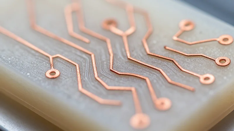
Teflon, or Polytetrafluoroethylene (PTFE), is the industry standard for high-frequency RF applications due to its exceptionally low dielectric constant (Dk) and low dissipation factor (Df). However, these electrical benefits introduce significant mechanical and thermal challenges during the PCB manufacturing process. Unlike standard FR-4 epoxy glass laminates, which are rigid and structurally consistent, PTFE-based materials are soft, flexible, and prone to significant dimensional changes when subjected to thermal cycles, making precision fabrication a high-stakes engineering endeavor.
Key Material Challenges and Manufacturing Implications
| Challenge | PTFE Behavior | Impact on Manufacturing |
|---|---|---|
| Dimensional Stability | High thermal expansion | Requires custom drill parameters and layer registration |
| Surface Energy | Extremely low adhesion | Demands specialized plasma etching/chemical treatment |
| Softness | Deforms under pressure | Requires specialized handling and copper weight management |
Critical Fabrication Requirements
To achieve the tolerances required for precision RF antennas, manufacturers must employ specialized preprocessing steps. Standard mechanical drilling often leads to 'smear' or delamination due to the heat generated by the drill bit. Consequently, advanced PCB houses utilize high-frequency plasma etching or complex sodium-naphthalene etching to modify the surface chemistry of the PTFE, ensuring copper traces adhere securely to the substrate. Furthermore, because PTFE is sensitive to heat, the lamination and curing cycles must be meticulously controlled to prevent internal stress that could warp the board or distort the impedance profile of antenna structures.
FAQ: Handling PTFE Substrates
- Why does PTFE require plasma treatment?
PTFE has inherently low surface energy, which prevents standard copper plating from adhering to the surface; plasma treatment modifies the polymer surface to allow for successful chemical bonding. - How does thermal expansion affect RF performance?
PTFE expands significantly with heat, which can shift the positioning of trace patterns and vias, leading to impedance discontinuities that degrade antenna signal efficiency. - Is standard mechanical drilling suitable for PTFE?
No, standard drilling often induces heat that melts the soft substrate, resulting in jagged hole walls and conductive contamination that ruins the integrity of the RF circuit.
Evaluating Dielectric Consistency and Material Stability

The Impact of Dielectric Constant (Dk) Stability
In high-frequency RF applications, even minor fluctuations in the dielectric constant (Dk) across the board surface can lead to catastrophic impedance mismatches. Because RF signals travel along the trace-dielectric interface, the Dk determines the signal velocity and phase consistency. For precision antenna arrays, a shift in Dk manifests as beam squint or pattern degradation, which is why selecting a manufacturer with robust Dk characterization is non-negotiable.
Comparing Material Stability Factors
| Parameter | Effect on RF Performance | Manufacturer Requirement |
|---|---|---|
| Dk Uniformity | Phase shift and impedance drift | Surface-to-surface variance < 0.02 |
| Thermal Stability | Coefficient of Thermal Expansion (CTE) mismatch | Consistent Tg and stable Dk over temperature |
| Moisture Absorption | Dielectric loss increase | Low-hygroscopic material processing |
Verifying Manufacturer Testing Protocols
A qualified manufacturer must go beyond simple incoming material inspection. They should demonstrate an active program for tracking batch-to-batch variations. Engineers should request evidence of how the fabricator handles board orientation and panel utilization to mitigate the impact of PTFE's inherent anisotropy.
- How do I verify Dk consistency?
Ask for the manufacturer's C-band or X-band resonant strip testing data, which confirms the actual Dk value at the specific frequency of your antenna operation. - Why does panel layout matter?
PTFE laminates often have glass-weave patterns. A manufacturer should use 'cut-to-weave' or optimized panelization techniques to ensure consistent RF trace impedance across the entire board surface. - What should I look for in the material certs?
Look for the supplier's Certificate of Conformance (CoC) that specifically cites the dielectric constant tolerance provided by the laminate manufacturer for that exact batch.
The Role of ISO Certification and Quality Management Systems
The Necessity of Certified Quality Systems
When sourcing for high-frequency precision RF antennas, documentation and process repeatability are as important as the physical fabrication. ISO 9001 serves as the foundational requirement for any reputable facility, ensuring that the manufacturer has established standardized operating procedures for every stage of the production cycle. For projects involving aerospace, defense, or critical telecommunications, seeking partners with AS9100 certification is highly recommended, as it imposes even stricter requirements for risk management, configuration control, and traceability.
Comparing Quality Standards in PCB Manufacturing
| Standard | Primary Focus | Relevance to RF Teflon PCBs |
|---|---|---|
| ISO 9001 | General Quality Management | Ensures consistent processes and documentation across all fabrication steps. |
| AS9100 | Aerospace & Defense Quality | Mandatory for high-reliability applications; adds strict traceability and risk assessment. |
| IPC-6012 | Rigid PCB Qualification | Provides specific performance classes (Class 2/3) for physical board integrity. |
Key Considerations for Quality Assurance
- How does ISO certification affect RF signal integrity?
A certified system guarantees that process parameters—such as etching tolerances and lamination temperatures—are locked in. This consistency is vital for maintaining the stable dielectric constant required to prevent phase shifts in RF antennas. - Is internal traceability enough?
No. For high-frequency projects, the manufacturer must provide material lot traceability from the copper-clad laminate supplier through to the final inspection, allowing you to correlate any performance issues back to specific material batches. - What should I look for in a quality audit?
Request their process control plan specifically for PTFE-based materials, focusing on how they mitigate mechanical stress and ensure registration accuracy during the multi-layer bonding process.
Ultimately, a manufacturer's adherence to these standards acts as a risk mitigation strategy. By choosing a partner with robust quality systems, you ensure that the laboratory-grade precision of your design is faithfully translated into a repeatable, high-performance antenna product.
Advanced Impedance Control Capabilities
Precision Etching and Trace Geometry Control
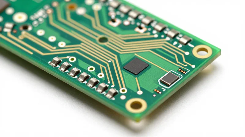
When working with Teflon (PTFE) substrates, standard PCB etching processes are insufficient due to the material's unique thermal expansion and bonding characteristics. Manufacturers must utilize chemical milling or precision laser-direct imaging (LDI) to maintain the exact trace widths required for impedance matching. Any deviation in the trace sidewall profile—such as undercutting or trapezoidal effects—will lead to unpredictable impedance spikes in high-frequency RF designs.
Verifying Impedance and Stack-up Integrity
To guarantee that the finished antenna performs as simulated, your manufacturer must employ Time Domain Reflectometry (TDR) testing directly on the production panel. Relying on coupon-based testing alone is often inadequate for complex PTFE multilayer structures where layer-to-layer registration can shift during lamination.
| Capability | Requirement for RF Precision | Manufacturer Validation |
|---|---|---|
| Trace Profiling | Vertical/Rectangular sidewalls to minimize skin effect. | Cross-section SEM imagery. |
| Dielectric Thickness | ±1-2% control to maintain target impedance. | Automated optical measurement reports. |
| Lamination Press | Controlled pressure and ramp rates for PTFE bonding. | Process log audits. |
Common Questions on Impedance Verification
- Why is TDR testing critical for RF antenna boards?
TDR provides a real-time visualization of impedance continuity along the transmission line, allowing the manufacturer to identify capacitive or inductive discontinuities caused by manufacturing defects. - How does the manufacturer account for copper surface roughness?
Advanced manufacturers use low-profile copper foils and incorporate roughness correction factors into their impedance modeling software to prevent signal attenuation at higher frequencies. - Should I request internal impedance coupons?
Yes, high-precision projects benefit from dedicated impedance coupons located on the PCB periphery, matching the layer stack-up and copper distribution of the primary antenna circuits.
Assessing Thermal Stability and Heat Management
Assessing Thermal Stability and Heat Management
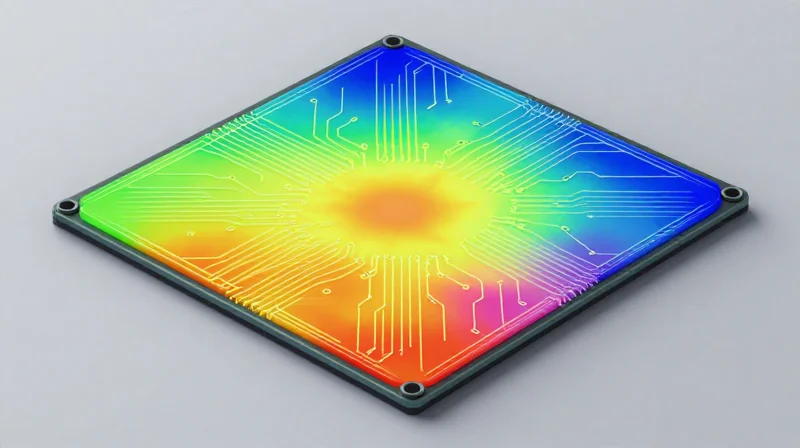
Teflon-based laminates, particularly PTFE, are prone to dimensional movement when exposed to thermal cycling. For high-frequency RF antenna projects, a manufacturer must demonstrate mastery over the Coefficient of Thermal Expansion (CTE) and the Thermal Coefficient of Dielectric Constant (TCDk). Selecting a partner who lacks the specialized equipment to characterize these parameters can result in frequency shifts and signal degradation as your antenna heats up during operation.
Key Thermal Metrics for Comparison
| Parameter | Significance for RF Antenna | Manufacturer Validation |
|---|---|---|
| CTE (Z-Axis) | Prevents barrel cracking in vias | Thermomechanical Analysis (TMA) |
| TCDk | Ensures resonant frequency stability | Resonant Cavity Testing |
| Tg (Glass Transition) | Defines structural rigidity limits | Differential Scanning Calorimetry (DSC) |
Technical FAQ: Thermal Management Capabilities
- Why is Z-axis expansion critical for Teflon PCBs?
PTFE laminates exhibit high Z-axis CTE; if the manufacturer cannot control the drill parameters and plating process, the resulting expansion can snap copper vias under thermal stress. - Does my manufacturer need in-house environmental chambers?
Ideally, yes. A high-tier manufacturer should perform thermal shock and cycling tests on prototype coupons to ensure the PCB stack-up behaves predictably before committing to full-scale production. - How does TCDk affect antenna performance?
The Dielectric Constant of PTFE varies with temperature. If the manufacturer does not account for this drift, your antenna's center frequency will shift unpredictably during high-power transmission.
When vetting candidates, prioritize manufacturers that utilize advanced simulation software like ANSYS HFSS or CST to model thermal-structural interaction. This predictive capability is a hallmark of a partner that understands the holistic relationship between material science and RF physics.
The Importance of Surface Finish and Copper Foil Selection
The Impact of Copper Foil Profiles on Skin Effect
At high frequencies, the skin effect restricts the majority of current flow to the outer surface of the copper conductor. Consequently, the surface roughness of the copper foil significantly influences signal loss. Standard electro-deposited (ED) copper, while cost-effective for general applications, features a rough profile that increases the effective path length for high-frequency signals, leading to higher insertion loss. For precision RF antennas, low-profile (LP) or very-low-profile (VLP) copper foils are essential to minimize these parasitic effects.
| Copper Type | Roughness Profile | RF Suitability | Primary Benefit |
|---|---|---|---|
| Standard ED | High | Low | Lower Cost |
| LP (Low Profile) | Medium | Moderate | Balanced |
| VLP (Very Low Profile) | Low | High | Minimal Signal Loss |
Surface Finish Selection for RF Reliability
The surface finish serves not only as a protective barrier against oxidation but also acts as a critical interface for signal transition. For Teflon-based substrates, the choice of finish must balance electrical performance with structural integrity. Finish flatness is paramount to ensure consistent impedance across the antenna geometry, particularly when dealing with fine-pitch components.
- Why is ENIG often avoided in ultra-high frequency designs?
While Electroless Nickel Immersion Gold (ENIG) offers excellent solderability and shelf life, the nickel layer is magnetic and exhibits higher loss at extreme frequencies, which can degrade performance compared to silver or gold-based alternatives. - Is Immersion Silver a viable alternative?
Immersion Silver (ImAg) provides a flatter surface and superior electrical performance compared to ENIG, making it a preferred choice for many RF applications, though it is susceptible to tarnishing if not handled correctly. - How does surface flatness affect signal integrity?
Any irregularities or non-uniformity in the surface finish can lead to impedance discontinuities. For high-precision RF antennas, a highly planar surface is non-negotiable to prevent reflections and phase shifts.
Verifying Manufacturing Throughput and Technical Support
Verifying Manufacturing Throughput and Scalability
For high-frequency RF projects, throughput capacity is not merely about raw volume; it is about the consistency of quality across production runs. A manufacturer must demonstrate clear metrics for cycle times while maintaining the rigid tolerances required for PTFE-based substrates. When vetting a partner, verify their ability to handle material procurement lead times, as specialized high-frequency laminates often face long delivery queues.
| Capacity Indicator | Why It Matters for RF | Verification Metric |
|---|---|---|
| Material Lead Times | Prevents project stalls. | Inventory turnover frequency. |
| Panel Yield Consistency | Reduces cost of scrapped PTFE. | Average first-pass yield rate. |
| Throughput Scalability | Ensures rapid prototyping. | Lead time for prototype vs. production. |
The Strategic Value of Dedicated RF Engineering Support
Beyond production capability, a manufacturer’s DFM (Design for Manufacturing) support team acts as an extension of your own engineering department. For complex RF antenna designs, having access to an RF-specialized engineer ensures that the transition from simulation to physical copper is seamless, addressing potential impedance discontinuities before they reach the shop floor.
- Why is a DFM review crucial before production?
A DFM review identifies potential issues with trace geometry, plating thickness, and stack-up symmetry, which are critical for preventing signal loss in high-frequency RF applications. - How does dedicated support accelerate time-to-market?
Direct communication with the manufacturer’s technical team eliminates the back-and-forth ambiguity that often leads to repeated design revisions and costly manufacturing delays. - What should I look for in a technical support team?
Look for manufacturers that provide real-time access to process engineers who have specific expertise in Teflon/PTFE handling, impedance modeling, and RF signal propagation.
Conducting a Facility Audit and Process Validation
The Necessity of On-Site Audits for PTFE Processes
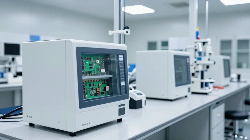
Teflon (PTFE) manufacturing requires highly specialized environmental controls and handling procedures distinct from standard FR-4 production. An on-site facility audit allows you to verify that the manufacturer maintains a cleanroom environment free from cross-contamination, which is critical for preventing signal degradation in RF applications. During your visit, assess their material storage logs to ensure PTFE laminates are stored under stable temperature and humidity conditions to prevent substrate warping or dielectric constant drift.
Process Validation Benchmarks
Beyond physical inspections, validating their internal quality control processes is paramount. You must demand proof of standardized RF testing protocols and detailed traceability from raw laminate lot number to the finished antenna structure.
| Audit Parameter | Requirement for RF Projects | Risk if Deficient |
|---|---|---|
| Plasma Etching Capability | Required for PTFE surface activation | Poor copper-to-dielectric adhesion |
| Drill Tolerance Control | Mechanical accuracy < 0.05mm | Impedance mismatch in via structures |
| Cleanroom Grade | ISO Class 7 or better | Dielectric contamination/signal noise |
| RF Simulation Integration | Direct CAD-to-CAM workflow | Design translation errors |
Frequently Asked Questions on Vetting
- How far back should historical performance data go?
Request at least two years of DFM audit reports specifically for PTFE-based RF projects to gauge their consistency in managing thermal expansion and impedance tolerances. - What is the most critical question to ask their engineering team?
Ask specifically how they mitigate the effects of 'drill smear' on PTFE substrates, as traditional mechanical desmear methods can severely damage high-frequency laminates. - Is a remote audit sufficient for RF manufacturers?
While virtual audits can review documentation, an on-site visit is mandatory to inspect the specific etching equipment and handling protocols required for specialized soft-substrate materials.
Selecting the right Teflon PCB manufacturer is a critical investment in your project's success, directly impacting signal integrity and overall antenna efficiency. By prioritizing material expertise, precise impedance control, and rigorous quality assurance, you can mitigate risk and ensure high-frequency performance. Ready to ensure your next RF project hits peak performance? Contact our engineering team today to discuss your PCB requirements.
