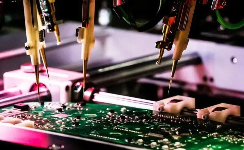
As the world increasingly embraces renewable energy, the demand for efficient and reliable energy storage solutions is skyrocketing. At the heart of these innovative systems lies the hybrid energy storage inverter, a critical component that seamlessly manages power flow between various sources and loads. But what truly powers these sophisticated devices? The answer lies in their robust Printed Circuit Boards (PCBs). Zero One Solution Limited, a leader in rapid-response PCB solutions, provides comprehensive one-stop services from design to manufacturing and assembly, ensuring your hybrid energy storage inverter projects achieve unparalleled performance and market readiness.
The Pivotal Role of PCBs in Hybrid Energy Storage Inverters
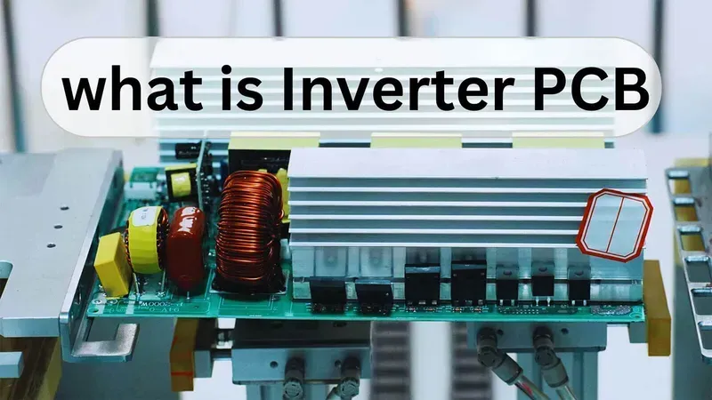
Hybrid Inverter PCB
At the core of every high-performance hybrid energy storage inverter lies the Printed Circuit Board (PCB), serving as the indispensable backbone that orchestrates the complex interplay of power conversion, intelligent control, and seamless communication. Far from being a mere circuit carrier, the PCB in these advanced systems is a sophisticated engineering marvel, enabling efficient energy flow between diverse sources—such as solar panels, batteries, and the grid—while ensuring robust system stability and longevity. Its precise design and superior manufacturing are paramount to achieving optimal performance, safeguarding against power losses, and ensuring reliable operation in demanding environments.
Optimizing Power Conversion Efficiency PCBs in hybrid inverters are engineered to minimize energy loss during AC/DC and DC/AC conversions, crucial for maximizing the overall system efficiency. This involves meticulous trace routing, optimal component placement, and the use of materials with low dielectric loss, directly impacting the inverter's ability to efficiently manage energy flow from various sources like solar panels and battery banks to the grid or loads. According to a study by the National Renewable Energy Laboratory (NREL), a 1% improvement in inverter efficiency can lead to significant energy savings over the system's lifespan.
Ensuring System Stability and Reliability The PCB's design dictates the inverter's resilience against electrical noise, thermal stress, and power fluctuations. Robust grounding schemes, effective thermal dissipation pathways, and careful impedance matching on the PCB are critical for preventing component degradation and ensuring stable operation. This stability is vital for critical infrastructure, where system downtime is unacceptable. For instance, data from the IEEE Power Electronics Society emphasizes that well-designed PCBs contribute significantly to a mean time between failures (MTBF) of over 100,000 hours for industrial power electronics.
Facilitating Advanced Communication Protocols Modern hybrid inverters require seamless communication between various sub-systems (e.g., battery management systems, grid synchronization units, and monitoring platforms). The PCB acts as the central nervous system, housing high-speed data lines and communication interfaces (like CAN bus, RS485, Ethernet) that enable real-time data exchange and remote control. This capability is essential for smart grid integration and demand-response applications, as highlighted by IEC 61850 standards for substation automation. Failure in PCB communication pathways can disrupt the entire energy management ecosystem.
Enhancing Thermal Management High-power components within inverters generate substantial heat, which can severely impact performance and lifespan if not properly managed. PCBs for hybrid inverters incorporate advanced thermal management techniques, such as thick copper layers, thermal vias, and specialized substrates (e.g., aluminum-backed PCBs or ceramic substrates), to efficiently dissipate heat away from critical components. Effective thermal design, as advised by JEDEC standards, can extend the lifespan of power semiconductors by up to 50%.
Enabling Compact and Scalable Designs With increasing demands for smaller footprints and higher power densities, the PCB plays a critical role in achieving compact inverter designs without compromising performance. Multi-layer PCBs, high-density interconnect (HDI) technology, and precise component placement allow for complex circuitry to be integrated into minimal space, facilitating easier installation and system scalability. This compact design is a key differentiator in competitive markets, offering installation flexibility in diverse applications from residential to utility-scale projects.
Key Design Considerations for Hybrid Inverter PCBs
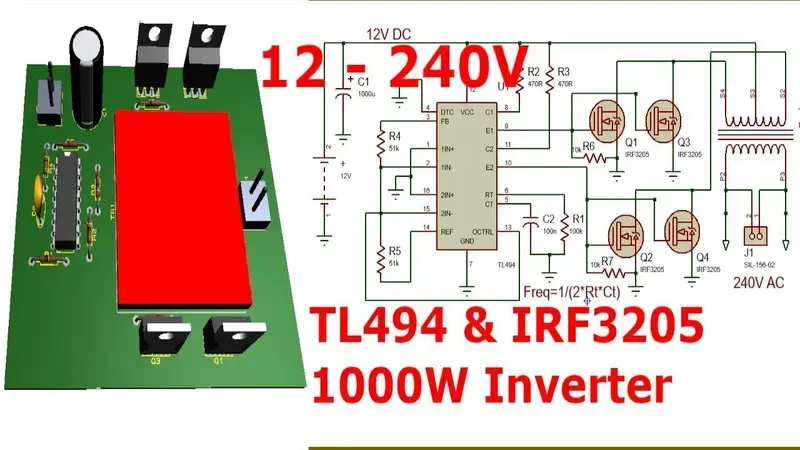
Inverter PCB Design High Current
Designing Printed Circuit Boards (PCBs) for hybrid energy storage inverters demands meticulous attention to specific engineering considerations that transcend typical PCB layouts. The core challenge lies in balancing the high power demands and complex control functionalities within a compact, reliable, and thermally stable architecture. Achieving this equilibrium is paramount for the inverter's efficiency, longevity, and its ability to seamlessly manage bidirectional power flow between diverse energy sources and loads.
High Current Path Optimization Hybrid inverters handle substantial power, necessitating robust current paths. This requires careful trace width and copper weight selection to minimize resistive losses (I²R) and prevent excessive heat generation. Multi-layered PCBs with dedicated power planes are often employed to distribute current efficiently and reduce impedance. Proper via selection and placement are also critical to ensure low resistance connections between layers and components, especially for high-current sections like DC bus connections and AC output lines.
Thermal Management Strategies Heat dissipation is a major concern due to the high power density. Effective thermal management involves strategic component placement (e.g., power semiconductors away from sensitive control circuitry), the use of thermal vias, copper pours, and in some cases, integrated heat sinks or liquid cooling channels within the PCB design. Simulation tools are crucial to predict hotspots and optimize thermal pathways, ensuring components operate within their safe temperature limits, thereby extending the inverter's lifespan and maintaining performance.
Design Aspect
Impact on Inverter Performance
Mitigation/Best Practice
EMI/EMC Compliance
Ensures stable operation by preventing interference with other electronic devices and minimizing self-interference. Critical for regulatory certification.
Beyond these, the integration of complex control circuits, often involving high-speed microcontrollers, DSPs, and communication interfaces (e.g., CAN, Ethernet), requires meticulous signal integrity management. This includes impedance matching, controlled impedance routing, and careful layout to minimize crosstalk and noise. The PCB design must also account for vibration resistance and environmental protection, especially for outdoor or industrial installations, often requiring conformal coatings or robust enclosures. Ultimately, these intricate design considerations are fundamental to unlocking the full potential and reliability of hybrid energy storage inverter systems.
Materials and Manufacturing Excellence for Inverter PCBs
PCB Material Manufacturing
The performance and longevity of a Hybrid Energy Storage Inverter PCB are critically dependent on the selection of advanced materials and the precision of manufacturing processes. For high-power applications, standard PCB materials often fall short, necessitating specialized substrates and fabrication techniques that can withstand extreme thermal loads, high current densities, and maintain signal integrity. Achieving manufacturing excellence in this domain means leveraging materials with superior dielectric properties and thermal conductivity, coupled with a robust production methodology that ensures defect-free boards capable of sustained, reliable operation in demanding energy storage environments.
Material Type
Key Properties for Inverter PCBs
Application Benefits
FR-4 (Enhanced)
Improved Tg, Low Dk/Df, Cost-effective
General-purpose, suitable for control circuits and lower power sections
Polyimide
High Tg, Excellent Thermal Stability, Chemical Resistance
RF/Microwave sections, high-speed data transmission
Copper Core/Heavy Copper
Superior Thermal Management, High Current Carrying Capacity
Power planes, heat sinks, high current paths in power stages
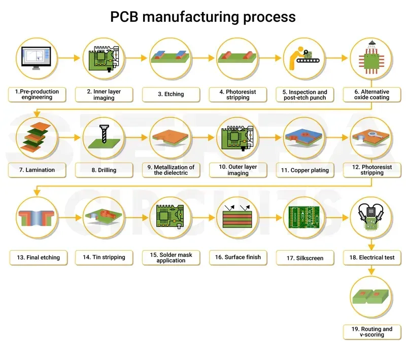
Advanced Manufacturing Processes for Hybrid Inverter PCBs Manufacturing Hybrid Inverter PCBs demands more than standard processes. It requires precision techniques such as advanced multilayer stacking for complex circuit integration, specialized via filling for enhanced thermal and electrical connectivity, and precise surface finishes (e.g., ENIG, ENEPIG) to ensure robust solderability and long-term reliability. Automation and stringent process control are paramount to meet the tight tolerances and high-quality standards required for these critical components. Furthermore, heavy copper plating is often employed to handle the significant current loads and dissipate heat effectively, ensuring the inverter's stable operation under peak demand.
Zero One Solution Limited: Your Strategic Partner in PCB Innovation
At the heart of every high-performance hybrid energy storage inverter lies a sophisticated Printed Circuit Board (PCB), and Zero One Solution Limited stands as a preeminent strategic partner in delivering cutting-edge PCB solutions specifically tailored for these demanding applications. Our comprehensive, one-stop service model, spanning from meticulous design optimization and rapid prototyping to efficient manufacturing and precise assembly, empowers innovators to accelerate their product development cycles and bring reliable, advanced hybrid energy storage systems to market with unparalleled speed and confidence. Leveraging over a decade of industry leadership, our expertise ensures that the critical PCB components of your inverter designs are not merely manufactured, but engineered for optimal performance, durability, and seamless integration within complex energy management ecosystems.
Full-Spectrum PCB Design and Optimization We offer holistic design review and optimization services, collaborating closely with your engineering teams to refine PCB layouts for enhanced power efficiency, thermal dissipation, signal integrity, and electromagnetic compatibility (EMC) crucial for hybrid inverter applications. Our DFM (Design for Manufacturability) and DFA (Design for Assembly) expertise proactively identifies and mitigates potential production challenges, ensuring a smooth transition from concept to mass production.
Rapid Prototyping for Accelerated Development Understanding the critical need for speed in the energy sector, our rapid prototyping capabilities enable quick iteration and validation of hybrid inverter PCB designs. This agile approach significantly compresses development timelines, allowing engineers to test performance, verify functionalities, and make necessary adjustments with unprecedented efficiency, minimizing costly delays and accelerating market entry.
Advanced Manufacturing Excellence Zero One Solution Limited utilizes state-of-the-art manufacturing processes and facilities to produce high-quality PCBs. For hybrid energy storage inverters, this includes precise fabrication of multi-layer boards, implementation of advanced material systems capable of handling high voltages and currents, and meticulous adherence to industry-leading IPC standards. Our commitment to precision ensures the robustness and longevity required for demanding energy applications.
Precision Assembly Services (PCBA) Beyond manufacturing, we provide comprehensive PCB assembly (PCBA) services, from component procurement and kitting to automated SMT (Surface Mount Technology) and through-hole assembly. Our experienced technicians ensure the accurate placement and soldering of all components, including power semiconductors and control ICs, critical for the reliable operation of hybrid inverters. Rigorous inspection and testing protocols are integrated at every stage to guarantee defect-free assemblies.
Strategic Global Supply Chain Management Headquartered in Shenzhen with a branch in Dubai, Zero One Solution Limited operates within a robust global PCBA supply chain network. This strategic positioning provides seamless access to a diverse range of high-quality components and raw materials, ensuring competitive pricing, reliable sourcing, and timely delivery, which are paramount for managing complex production schedules for hybrid energy storage solutions.
Service Area
Zero One Solution Limited Capability
Benefit for Hybrid Inverter PCBs
Design Optimization
DFM/DFA analysis, thermal simulation, signal integrity analysis
Reduces development cycles, improves performance, minimizes errors
Prototyping Speed
1-3 day rapid PCB prototyping
Accelerates design validation and time-to-market
Material Expertise
Specialized high-Tg, low-loss laminates, heavy copper options
Ensures thermal stability, high current handling, long-term reliability
Ensures cost-effectiveness and material availability
Accelerating Development with Rapid Prototyping Services
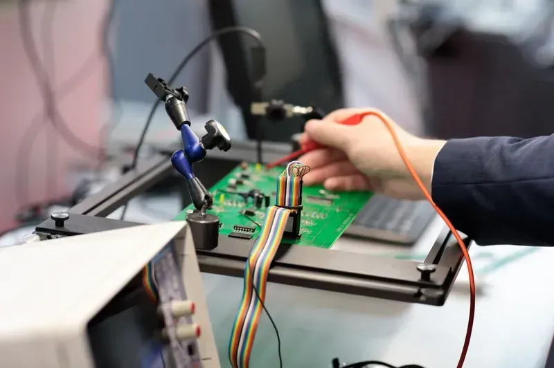
PCB Prototype Testing
Rapid prototyping is an indispensable cornerstone in the swift and efficient development of Hybrid Energy Storage Inverter PCB solutions, empowering engineers to transform innovative concepts into tangible, testable hardware with unprecedented speed. This accelerated iteration capability is critical for validating complex power management circuits, optimizing thermal performance, and ensuring electromagnetic compatibility in real-world scenarios. By compressing the design-test-refine cycle, rapid prototyping not only de-risks product development but also significantly reduces the time-to-market for cutting-edge energy storage systems, giving businesses a crucial competitive edge in the rapidly evolving renewable energy landscape.
Expedited Design Validation Rapid prototyping allows for immediate physical realization of design iterations, enabling engineers to quickly validate circuit functionalities, component placements, and signal integrity of hybrid inverter PCBs under operational conditions. This early detection of potential issues prevents costly redesigns further down the development pipeline, optimizing the entire process.
Optimized Performance and Efficiency Through rapid prototyping, various design parameters for hybrid inverter PCBs, such as power path impedance, thermal dissipation strategies, and high-frequency noise suppression, can be empirically tested and refined. This iterative process leads to superior performance, enhanced efficiency, and greater reliability of the final product, directly impacting energy conversion and storage effectiveness.
Reduced Time-to-Market In the fast-paced energy sector, time-to-market is a critical differentiator. Zero One Solution Limited's rapid prototyping services drastically cut down the lead times for PCB fabrication and assembly, allowing clients to transition from concept to market-ready product in a fraction of the traditional timeline. This agility is vital for capitalizing on emerging market demands and technological advancements.
Cost-Effective Iteration and Risk Mitigation Prototyping in early stages with rapid turnaround times minimizes the financial risk associated with design flaws. By identifying and rectifying issues before mass production, companies avoid expensive retooling and material waste. This iterative approach is far more cost-effective than discovering problems during large-scale manufacturing runs.
Prototyping Metric
Traditional PCB Development
Zero One Solution Rapid Prototyping
Design-to-Prototype Lead Time
3-6 weeks
3-7 days
Iteration Cycles
Limited due to time/cost
Multiple, continuous
Risk of Late-Stage Design Flaws
High
Low
Overall Development Cost
Higher (due to reworks)
Lower (optimized iterations)
Quality Assurance and Testing for Reliable Inverter PCBs
PCB Quality Control
Ensuring the unwavering reliability and longevity of hybrid energy storage inverter PCBs is paramount, and at Zero One Solution Limited, this is achieved through a multi-faceted approach to quality assurance and rigorous testing protocols that meticulously validate every board. Our commitment extends beyond mere functionality, focusing on performance under demanding conditions to guarantee sustained operation in critical energy management systems. This dedication to precision and durability is fundamental to the successful deployment of advanced inverter technologies, providing the foundational stability required for efficient energy conversion and storage.
Testing Phase
Description
Objective
Key Equipment/Methods
Design Review (DFM/DFA)
Early-stage analysis of PCB designs for manufacturability and assembly efficiency.
Identify and mitigate potential manufacturing issues before production begins, ensuring cost-effectiveness and quality.
Future Trends in Hybrid Energy Storage and PCB Evolution
The landscape of hybrid energy storage is rapidly evolving, driven by the imperative for sustainable energy solutions and grid resilience. This evolution directly impacts the design and manufacturing of Printed Circuit Boards (PCBs), necessitating advancements that can accommodate higher power densities, intelligent grid integration, and the complexities introduced by artificial intelligence (AI) and machine learning (ML) in energy management systems. The future demands PCBs that are not only robust and efficient but also adaptable to the dynamic requirements of next-generation energy ecosystems.
Enhanced Power Density and Miniaturization Future hybrid energy storage systems will demand even higher power densities within smaller footprints. This trend will push PCB manufacturers to explore advanced substrate materials with superior thermal conductivity, higher dielectric constants, and finer trace/space capabilities. Technologies like High-Density Interconnect (HDI) PCBs and even 3D PCB architectures will become more prevalent, enabling greater component integration and reduced physical size without compromising performance. For instance, the adoption of gallium nitride (GaN) and silicon carbide (SiC) power devices, known for their high switching speeds and efficiency, necessitates PCBs capable of handling ultra-fast transient responses and minimizing parasitic inductances, often requiring specialized laminate materials and precise impedance control.
Smarter Grid Integration and Communication The integration of hybrid energy storage with smart grids is paramount for optimizing energy flow, ensuring grid stability, and enabling demand response. This requires PCBs to incorporate sophisticated communication interfaces (e.g., Modbus, Ethernet, Wi-Fi, 5G) and advanced microcontrollers capable of processing complex algorithms for real-time data analysis and predictive control. Future PCBs will feature enhanced electromagnetic compatibility (EMC) to prevent interference in densely packed electronic environments, ensuring reliable data transmission and robust operation within interconnected smart energy networks. This also includes the burgeoning field of Vehicle-to-Grid (V2G) technology, where electric vehicle batteries act as distributed energy storage, requiring even more robust and intelligent PCB solutions for bidirectional power flow.
Artificial Intelligence and Machine Learning Integration AI and ML algorithms are increasingly being deployed to optimize energy dispatch, predict consumption patterns, and enhance the lifespan of battery systems within hybrid storage solutions. This necessitates PCBs that can host powerful embedded processors, dedicated AI accelerators, and ample memory for executing these complex algorithms directly on the inverter. The design focus will shift towards creating PCBs that facilitate high-speed data transfer between sensors, power stages, and processing units, potentially incorporating specialized routing for neural network architectures or dedicated tensor processing units (TPUs) to handle the computational demands of AI/ML, thereby improving efficiency and reducing reliance on cloud-based processing for critical functions.
Modular and Scalable PCB Designs To meet diverse application needs and facilitate future upgrades, there will be an increasing emphasis on modular and scalable PCB designs. This approach allows for easier customization, expansion, and maintenance of hybrid energy storage systems. PCBs will be designed with standardized interfaces and potentially hot-swappable modules for various functionalities (e.g., battery management, grid synchronization, DC/DC conversion), reducing downtime and improving the overall flexibility of the system. This modularity also simplifies manufacturing and assembly processes, leading to cost efficiencies and faster time-to-market for new configurations.
Enhanced Reliability and Lifecycle Management As hybrid energy storage systems become critical infrastructure, the reliability and longevity of their PCBs are paramount. Future trends include advanced prognostics and health management (PHM) capabilities embedded within the PCB design, allowing for real-time monitoring of component health and predictive maintenance. This involves integrating more sensors (temperature, current, voltage) and robust data logging capabilities directly onto the board. Furthermore, the focus on sustainable manufacturing practices and the use of eco-friendly materials will gain prominence, aiming to reduce the environmental footprint throughout the PCB's lifecycle, from production to end-of-life recycling, aligning with global sustainability goals.
FAQs: Hybrid Energy Storage Inverter PCB Solutions
What are the primary design challenges for Hybrid Energy Storage Inverter PCBs? Designing PCBs for hybrid energy storage inverters presents unique challenges, primarily due to the need to handle high power densities, manage significant heat dissipation, and ensure robust electromagnetic compatibility (EMC). These inverters must efficiently convert and manage power flows between diverse sources like solar panels, batteries, and the grid, demanding high current carrying capabilities and precise signal integrity. Additionally, compact form factors necessitate innovative thermal management solutions to prevent component degradation and ensure long-term reliability. Meeting stringent safety standards and integrating complex control algorithms also adds layers of complexity to the PCB layout and component selection.
How does Zero One Solution Limited ensure the reliability and longevity of Inverter PCBs? Zero One Solution Limited prioritizes reliability and longevity through a multi-faceted approach. We employ rigorous material selection, opting for high-Tg laminates and robust copper weights capable of withstanding extreme thermal and electrical stresses. Our manufacturing processes adhere to IPC standards, utilizing advanced fabrication techniques for precise etching and robust solder joints. Furthermore, every Hybrid Energy Storage Inverter PCB undergoes extensive quality assurance protocols, including automated optical inspection (AOI), in-circuit testing (ICT), functional testing, and environmental stress screening (ESS) to identify and mitigate potential failure points before deployment, ensuring superior performance and durability in demanding applications.
What advanced manufacturing capabilities are crucial for Hybrid Inverter PCBs? Advanced manufacturing capabilities are crucial for producing high-performance Hybrid Inverter PCBs. These include multi-layer board fabrication for complex circuit integration, heavy copper plating for high current paths, and specialized thermal management features like embedded heat sinks or thermal vias. Precision drilling and routing, impedance control, and advanced surface finishes (e.g., ENIG, OSP) are also vital for signal integrity and component reliability. Our state-of-the-art facilities are equipped for high-mix, low-volume rapid prototyping as well as high-volume production, ensuring that even the most intricate designs are manufactured to the highest standards, crucial for the demanding environment of hybrid energy storage systems.
What are the key benefits of partnering with a specialized PCB provider like Zero One Solution Limited for Hybrid Energy Storage Inverter solutions? Partnering with Zero One Solution Limited offers several key benefits for Hybrid Energy Storage Inverter solutions. Our specialization ensures access to deep expertise in high-power electronics, rapid prototyping services that significantly accelerate product development cycles, and a comprehensive one-stop solution from design optimization to manufacturing and assembly. This integrated approach reduces supply chain complexities and improves overall project efficiency. Furthermore, our rigorous quality assurance processes and strategic global presence ensure consistent quality, cost-effectiveness, and seamless access to resources, enabling our clients to bring innovative and reliable hybrid inverter products to market faster and with greater confidence.
How do PCBs contribute to the efficiency of Hybrid Energy Storage Inverters? PCBs are fundamental to the efficiency of Hybrid Energy Storage Inverters by optimizing power flow and minimizing energy losses. High-quality PCBs with optimized layouts, appropriate trace widths, and proper grounding significantly reduce resistance and inductance, thereby minimizing I²R losses and electromagnetic interference (EMI). The strategic placement of components, especially power switching devices and magnetic elements, ensures efficient heat dissipation, preventing thermal runaway and maintaining optimal operating temperatures. Furthermore, the integration of high-speed digital control circuits on the PCB facilitates precise management of power conversion stages, dynamic load balancing, and overall system optimization, all contributing to maximum energy efficiency and prolonged system lifespan.
In conclusion, the success of hybrid energy storage inverters hinges significantly on the quality and precision of their underlying PCB solutions. Zero One Solution Limited stands as your premier partner, offering unparalleled expertise from rapid prototyping to full-scale manufacturing and assembly. Our commitment to quality, efficiency, and innovation ensures that your energy storage solutions are not just functional, but truly transformative. Partner with us to accelerate your product development cycle, reduce time-to-market, and contribute to a more sustainable energy future. Contact Zero One Solution Limited today to discuss your Hybrid Energy Storage Inverter PCB Solution needs and let us power your next breakthrough.