From the humble radio to the sophisticated circuits in our smartphones, transistors are the unsung heroes of modern electronics. Among them, the JFET transistor, or Junction Field-Effect Transistor, stands out for its unique voltage-controlled operation. This article delves into the heart of JFET technology, exploring its working principles, characteristics, and diverse applications, while demystifying its importance for both seasoned engineers and curious minds.
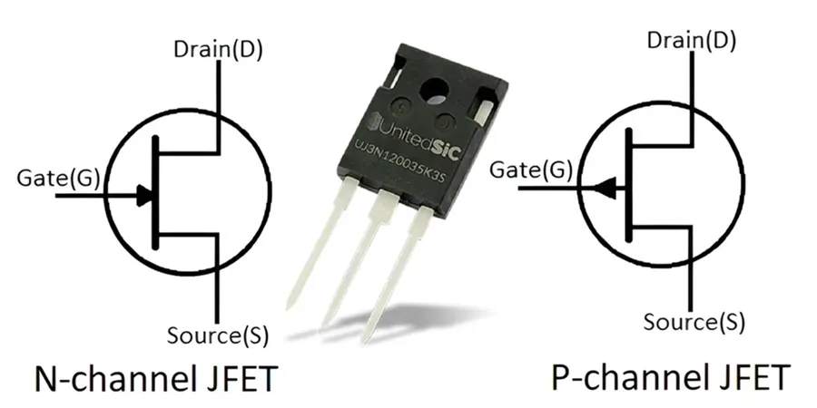
Junction Field-Effect Transistors (JFETs) are unipolar, voltage-controlled devices distinguished by their control of current flow through a channel via an applied gate voltage. Unlike bipolar junction transistors (BJTs) which rely on both electron and hole currents, JFETs operate using only one type of charge carrier, making them fundamentally different in structure and behavior.
JFETs possess three terminals: the source, drain, and gate. The source and drain are connected by a conductive channel, while the gate is positioned to modulate the channel's conductivity. This modulation is achieved by varying the gate voltage, which changes the depletion region within the channel, thereby controlling the current flow. The unipolar nature means JFETs are inherently less noisy than BJT's in certain applications.
| Feature | JFET | BJT |
|---|---|---|
| Charge Carriers | Unipolar (either electrons or holes) | Bipolar (both electrons and holes) |
| Control Mechanism | Voltage controlled | Current controlled |
| Input Impedance | High | Low |
| Noise Performance | Generally lower | Generally higher |
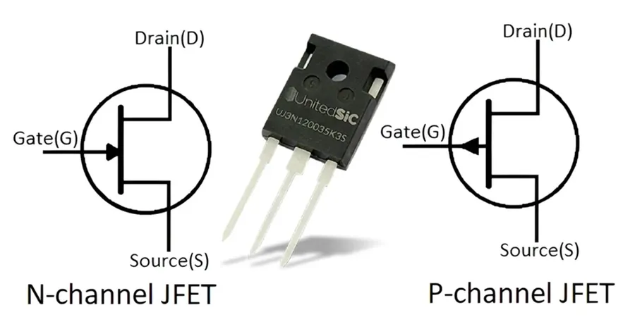
Junction Field-Effect Transistors (JFETs) are unipolar devices, meaning their current conduction relies primarily on one type of charge carrier (either electrons or holes). Understanding their physical structure is crucial to grasping their operational characteristics. JFETs are constructed with a channel made of a semiconductor material that allows current to flow from the source to the drain. The gate region, which surrounds the channel, modulates this current flow through the application of an electric field. The type of semiconductor material used dictates whether the JFET is an N-channel or a P-channel device.
| Feature | N-Channel JFET | P-Channel JFET |
|---|---|---|
| Majority Carriers | Electrons | Holes |
| Channel Material | N-type Semiconductor | P-type Semiconductor |
| Gate Voltage for Depletion | Negative relative to source | Positive relative to source |
| Current Direction (conventional) | Source to Drain | Drain to Source |
The key structural components of a JFET include the source, drain, and gate terminals. The source and drain are located at opposite ends of the channel. The gate is designed to control the current flow in the channel, forming a PN junction with the channel. The type of doping in the channel determines whether the JFET is an N-channel or P-channel type, influencing the polarity of the gate voltage required for operation. This structural distinction leads to notable differences in device characteristics.
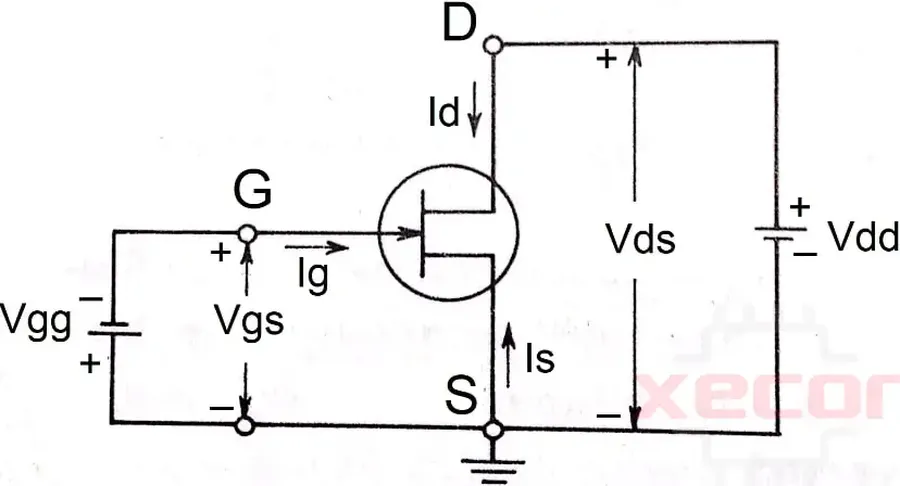
Junction Field-Effect Transistors (JFETs) are unipolar devices, meaning their current flow is controlled by a single type of charge carrier (either electrons or holes). The operation of a JFET hinges on the manipulation of a conductive channel's width through an applied gate voltage, thereby controlling the current between the source and drain terminals.
The core principle behind JFET operation is the modulation of the channel's conductance via the depletion region. A reverse bias voltage applied between the gate and source terminals creates a depletion region within the channel. This region, devoid of mobile charge carriers, effectively narrows the conductive channel. As the gate voltage is increased (more negative for an N-channel JFET, more positive for a P-channel JFET), the depletion region widens, further restricting current flow between the source and drain.
Crucially, JFETs are 'normally-on' devices. This means that when the gate voltage is zero, a maximum current (known as the drain-source saturation current, or Idss) flows from the source to the drain. Applying a gate voltage in the correct polarity reduces the channel width and thus the current flow. The gate voltage needed to completely close off the channel and prevent any drain current from flowing is called the pinch-off voltage (Vp). Beyond the pinch-off voltage, the current is nearly zero. In essence, the JFET operates as a voltage-controlled current source.
Unlike bipolar junction transistors (BJTs) which are current-controlled devices, JFETs are voltage-controlled, rendering them advantageous in applications requiring high input impedance and low noise operation.
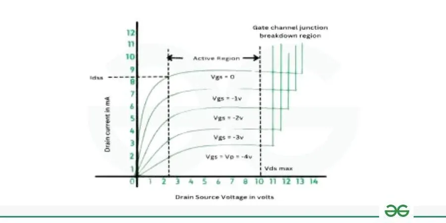
Understanding the current-voltage (I-V) characteristics of a Junction Field-Effect Transistor (JFET) is crucial for effective circuit design. These characteristics, typically represented graphically as I-V curves, reveal how the drain current (Id) responds to variations in drain-source voltage (Vds) and gate-source voltage (Vgs). Analyzing these curves and key parameters like transconductance (gm), drain current at zero gate voltage (Idss), and pinch-off voltage (Vp), provides engineers with the necessary insight to utilize the JFET's unique capabilities.
| Parameter | Symbol | Description | Significance |
|---|---|---|---|
| Transconductance | gm | The change in drain current (Id) for a given change in gate-source voltage (Vgs), with Vds constant. | Indicates the JFET's amplification capability and its sensitivity to the input signal. Crucial in amplifier design. |
| Drain Current at Vgs=0 | Idss | The drain current (Id) when the gate-source voltage (Vgs) is zero. Represents the maximum current the JFET can conduct. | A key indicator of the JFET's maximum current handling capability. Used in setting bias points. |
| Pinch-off Voltage | Vp | The gate-source voltage (Vgs) that causes the drain current to reduce to nearly zero. Marks the beginning of the saturation region. | Defines the operating region of the JFET and is essential for biasing and preventing saturation. |
The I-V characteristic curve for a JFET is distinctly segmented into two operating regions: the ohmic or linear region, and the saturation or active region. In the ohmic region, the JFET operates as a voltage-controlled resistor, and the drain current increases linearly with the drain-source voltage. As the Vds increases, the depletion region around the gate expands, and at a certain point the device enters the saturation region, where the drain current remains relatively constant despite the increases in Vds. The value of the Vds at which this occurs depends on the value of Vgs, and the shape of the I-V curves is modulated by the gate-source voltage.
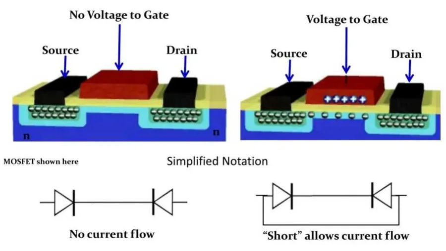
JFETs (Junction Field-Effect Transistors) and MOSFETs (Metal-Oxide-Semiconductor Field-Effect Transistors) are both field-effect transistors, but they differ significantly in their structure, operation, and characteristics, leading to varied applications. The fundamental distinction lies in the gate's structure and its control over the channel.
| Feature | JFET | MOSFET |
|---|---|---|
| Gate Structure | Reverse-biased P-N junction | Metal-Oxide-Semiconductor (Capacitor-like) |
| Gate Current | Very low (leakage current) | Extremely low (negligible) |
| Input Impedance | High | Very High |
| Channel Control | Depletion mode only | Enhancement or Depletion mode |
| Fabrication Complexity | Less complex | More complex |
| Switching Speed | Generally slower | Generally faster |
| Temperature Sensitivity | More susceptible to temperature variations | Less susceptible to temperature variations |
| Noise Performance | Good noise performance at low frequencies | Potentially higher noise |
| Applications | Analog circuits, low-noise amplifiers, voltage-controlled resistors | Digital circuits, high-speed switching, power electronics, logic gates, microprocessors |
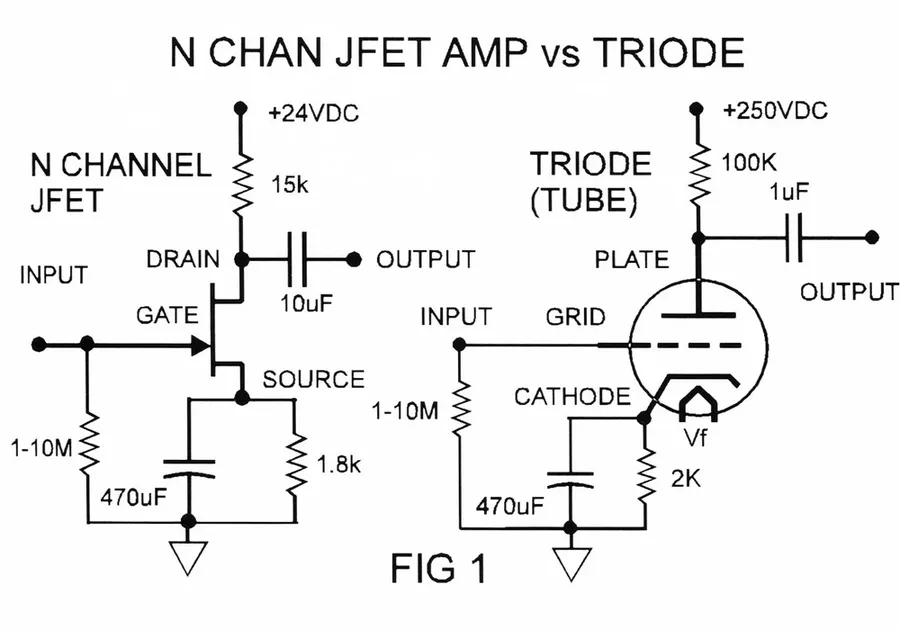
JFETs, owing to their voltage-controlled current characteristics, find extensive use in various electronic circuits. Their high input impedance, low noise, and simple biasing make them ideal for a multitude of applications, from amplification to switching and impedance matching.
The selection of the appropriate JFET for a specific application depends on factors such as the required gain, noise performance, operating frequency, and power dissipation. Understanding the trade-offs between different JFET parameters is essential for effective design of electronic circuits.
This section addresses common queries regarding JFET transistors, offering concise explanations to enhance understanding of their characteristics and applications. The questions cover key areas such as comparison with MOSFETs, their general purpose and limitations.
Successfully integrating JFET transistors into circuit designs requires careful attention to several practical considerations. These include implementing appropriate biasing techniques, understanding temperature-dependent behavior, managing noise contributions, and selecting the optimal JFET device for a given application. This section provides guidance on each of these crucial aspects.
The JFET transistor, a fundamental component in electronics, showcases the power of voltage-controlled current modulation. This article has explored the core workings, characteristics, and various applications of the JFET, highlighting its importance in diverse electronic circuits. From amplifying faint signals to acting as precise switches, the JFET continues to be a cornerstone of modern technology. Understanding the JFET's strengths, limitations, and how it stacks up against other transistor types like the MOSFET empowers engineers to make informed choices in their designs, further paving the way for technological innovation.

